Introduction
Insertion loss, the term used to express a filter’s ability to reduce or attenuate unwanted signals, has traditionally been measured in a 50 ohm source and 50 ohm load impedance condition, as standardized in MIL-STD-220.
In this matched 50 ohm impedance condition, various types of filter circuit configurations, single capacitor, “L’s”, “PI’s”, and “T’s”, will exhibit the same response for that given circuit regardless of the relationship between the input, output, and RF signal source.
MIL-STD-220 insertion loss tests are well defined, universal, and are excellent for monitoring filter manufacturing consistencies. However, the results can be misleading when it comes to selecting the proper filter circuit that must function in a complex impedance setting.
Passive inductive and capacitive filters are impedance sensitive devices by nature and therefore source and load conditions must be taken into consideration when selecting a filter circuit.
This is particularly true, and becomes more pronounced, when you consider that most EMI line filters are not matched filter networks. That is to say the ideal design value of the individual components that make up the network have been modified, or intentionally mismatched, in order to accommodate operating line voltages, operating line currents, and reasonable packaging schemes.
In most cases the ideal inductor for a given response has been greatly reduced in value to accommodate the operating current and reduce the DCR; therefore the capacitors have to be increased in value to achieve the required insertion loss.
This intentional mismatch, which is widely practiced throughout the industry, only affects the very low frequencies by introducing ripple in the pass-band and has little, if any, negative effect in the reject band.
Circuit Configurations
EMI line filters are passive devices and their effect are bidirectional. They are all low-pass brute force networks, passing DC and power line frequencies with very low losses while attenuating the unwanted signals at higher frequencies.
They do not differentiate between EMI generated inside or outside the subsystem or system. They are equally effective in reducing EMI emissions as well as protecting a device from unwanted EMI entering via the power lines.
Each additional element improves the slope of the insertion loss curve. That is, the reject-band will be reached must faster with each section, or element, added. Increasing or decreasing the individual elements values does not change the slope of the curve but does affect the cutoff frequency.
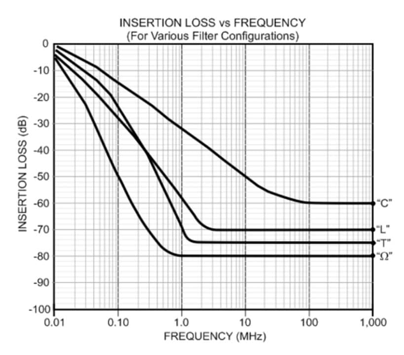
More importantly, when the source and load impedance of the circuit changes, the slope of the insertion loss curve also changes. A “PI” circuit type filter, for example, is best suited when the source and load impedances are of similar values and relatively high. As these impedances become lower, the insertion loss for the “PI” filter also becomes lower. The reverse is true for “T” circuits.
If the circuit impedances varies with frequency, as most circuits do, then it is advantageous to use multiple element filters such as a “PI” or “T” circuit. In the case of a “PI” circuit that exhibits maximum or load impedance is reduced the filter still has two active elements. For all practical purposes it becomes an “L” circuit.
Additionally, the amount of filtering achievable is limited by the inductance (ESL) and resistance (ESR) in the capacitor and the parasitic capacitance in the inductors. The results are that the insertion loss curves “levels off” at approximately 80 to 90 dB.
The following is a brief description of the most popular types of EMI Filter circuits and their application. It should be pointed out that these are only general guidelines due to the fact that most impedance conditions and EMI profiles are dynamic, complex, and change with frequency.
- Feedthrough Capacitor – A single element shunt feedthrough capacitor has attenuation characteristics that increases at a rate of 20 dB per decade (10 dB at 10 kHz, 30 dB at 100 kHz). A feedthrough capacitor filter is usually the best choice for filtering lines that exhibit very high source and load impedances.
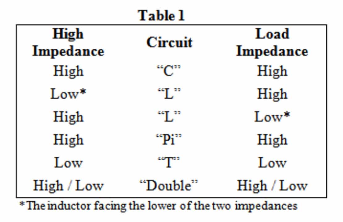
- L-Circuit Filter – A two element network consisting of a series inductive component connected to a shunt feedthrough capacitor. This type of filter network has attenuation characteristics that increases at a rate of 40 dB per decade (20 dB at 100 kHz, 60 dB at 1MHz). An “L” circuit filter is best suited for filtering lines when the source and load impedances exhibit large differences. For most applications this type of network provides the greatest performance when the inductor is facing the lower of the two impedances.
- PI-Circuit Filter – This is a three element filter consisting of two shunt feedthrough capacitors with a series inductive component connected between them. This three element filter has attenuation characteristics that increases at a rate of 60 dB per decade (20 dB at 15 kHz, 80 dB at 150 kHz). A “PI” circuit filter is usually the best choice when high levels of attenuation are required and when the source and load impedances are of similar values and relatively high.
- T-Circuit Filter – This also is a three element filter consisting of two inductive components with a single shunt feedthrough capacitors connected between them. Like the “PI” circuit filter, this device has attenuation characteristics that also increase at a rate of 60 dB per decade (20 dB at 15 kHz, 80 dB at 150 kHz). A “T” circuit filter is the best choice when high levels of attenuation are required and when the source and load impedances are of similar values and relatively low.
- Double Circuits – Double “L’s,” double “PI’s”, and double “T’s” consisting of four and five elements are best suited when extremely high levels of attenuation are required. Double “L’s” have a theoretical attenuation of 80 dB per decade, while double “PI’s” and double “T’s” have a theoretical attenuation of 100 dB per decade. The source and load impedance conditions that apply to the single circuit devices apply to the double circuit filters.
The following table summarizes the various source and load impedance settings and the proper filter circuit for that condition.
Mismatching
As previously stated, most EMI line filters are intentionally mismatched for ease in manufacturing. A typical example of this industry wide practice is a cylindrical style filter.
The military specifications for this particular filter are:
Operating Voltage: 70 VDC
Operating Current: 5 ADC
Circuit Configuration: “PI”
DC Resistance: .015 ohms maximum
Case Diameter: .410 inches maximum
Full Load Insertion Loss per MIL-STD-220 (50 ohms):
150 kHz: 16 dB
300 kHz: 38 dB
1 MHz: 75 dB
10 MHz: 80 dB
100 MHz: 80 dB
Based on a source and load impedance of 50 ohms, MIL-STD-220, a properly designed Butterworth filter (a filter network that has a maximum flat pass-band with average cutoff frequency to reject-band ratio), would produce the following element values in order to satisfy the minimum insertion loss requirements:
C1 = .0769 µfd
L2 = 385 µHy
C3 = .0769 µfd
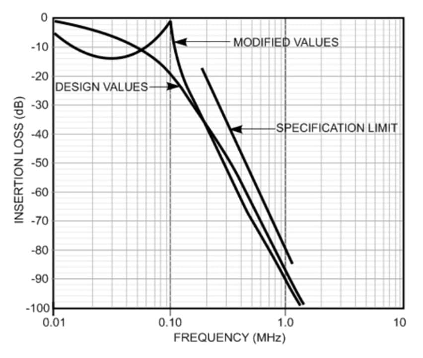
The theoretical MIL-STD-220 insertion for a “PI” filter of these values is as indicated below:
150 kHz: 33 dB
300 kHz: 51 dB
1 MHz: 83 dB
10 MHz: >100 dB
100 MHz: >100 dB
The capacitance values for C1 and C3, .0769 µfd, are acceptable for a 70 VDC rated filter and are easily manufactured. However, L2 must be 385 µHy in order to satisfy the insertion loss requirements
In order to achieve 385 µHy at 5 ADC, allow for core saturation (the change in incremental permeability of the core material with DC bias), and comply with the .015 DC resistance requirement, the diameter of the inductor would be in excess of 2.0 inches. This inductor would obviously not fit a case with an outside diameter of .410 inches.
By simply reducing the inductor to a realistic value and increasing the value of C1 and C3, we can achieve the required insertion loss in the reject-band with a design that can easily be manufactured. The typical values for this application would be:
C1 = .70 µfd
L2 = 5 µHy
C3 = .7 µfd
The theoretical MIL-STD-220 insertion for this modified filter is:
150 kHz: 25 dB
300 kHz: 50 dB
1 MHz: 83 dB
10 MHz: >100 dB
100 MHz: >100 dB
As previously stated, this practice of intentionally mismatching the element values will introduce a substantial amount of ripple, as much as 10 to 20 dB, in the pass-band. However, at frequencies below 1 KHz, the response is normally flat to within ± 1 dB.
Figure 2 depicts the MIL-STD-220 insertion loss characteristics for the ideal filter network and the modified design as compared to the specification requirements.
MIL-STD-220 Insertion Loss Verses MIL-STD-461 EMI Testing
The majority of EMI filters are employed in order to cause system compliance to one of various military or commercial EMI/EMC specifications.
The most widely references military EMI/EMC specification is Military Specification MIL-STD-461 (462,463). This document specifies the allowable amount of conducted and radiated emissions that a subsystem or system can generate.
Conducted emissions is interference that is present, or ‘conducted’ on primary power lines (AC or DC) and/or signal lines as detected by a current probe or other means.
Radiated emissions is interference, both ‘E” and “H” fields, that is being transmitted or radiated from the total system as detected by a receiving antenna.
In addition, MIL-STD-461 also delineates a series of tests that subject the device under test to various types of conducted and radiated interference to determine the survivability of the device when exposed to a harsh EMI environment. This series of tests is referred to as conducted and radiated susceptibility.
Conducted emission requirements and test methods are referred to as “CE”. The numbers that follow refer to the applicable frequency range and whether it pertains to input power lines or signal lines. (i.e., CE03 establishes test methods and maximum allowable interference that can be present on AC and DC power lines over the frequency range of 15 kHz to 50 MHz.)
Similarly, “CS” stands for Conducted Susceptibility, “RE” for Radiated Emission, and “RS” for Radiated Susceptibility.
As previously stated, EMI filters being bidirectional devices not only help to reduce the amount of conducted emissions generated within, but also protect the system from unwanted interference entering via the power lines and signal lines.
To some degree EMI filters also help to reduce the radiated interference. This is due to the fact that the power lines and signal lines can act as ‘transmitting antennas’ if too much EMI is present. However, the majority of radiated problems are system configuration related (i.e., improper grounding, shielding, lack of EMI gaskets, the choice of materials in the case of “H” fields, etc.).
The EMI profiles, and impedance, of any device is very complex and will change drastically over a given frequency range. It’s this phenomenon that makes selecting an EMI filter based solely on 50 ohm insertion loss data difficult.
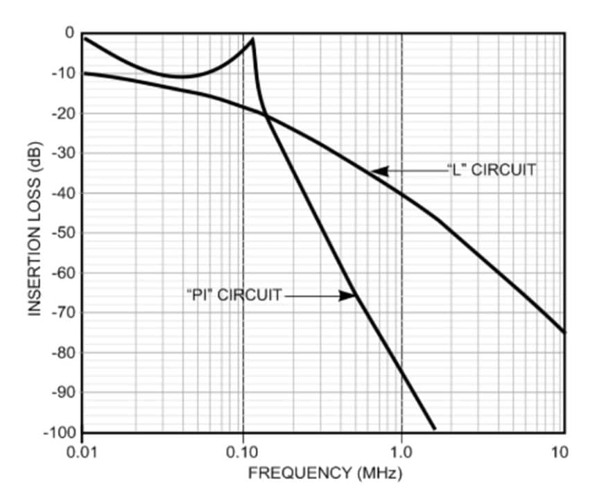
Figure 3 compares the theoretical MIL-STD-220 50 ohm insertion loss of a “PI” filter and a “L” filter comprised of the following components.
“PI” Circuit:
C1 = .70 µfd
L2 = 5 µHy
C3 = .70 µfd
“L” Circuit:
C1 = .70 µfd
L2 = 5 µHy
Looking at this comparison, and if size was not an issue, one would have a tendency to choose the “PI” circuit over the “L” circuit based on performance. At 1 MHz the “PI” circuit provides 80+ dB of insertion loss where the “L” circuit only provides 40+ dB.
However, MIL-STD-461 conducted emission tests are not performance under 50 ohm source and load conditions.
Figure 4 illustrates a typical MIL-STD-461 conducted emissions test configuration.
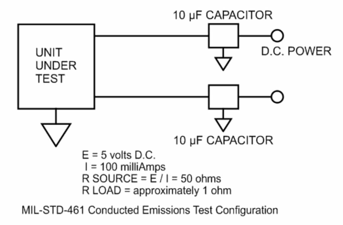
Not knowing the EMI source impedance (the device under test), we will assume ohms law. In this case 50 ohms. We don’t know what the load impedance is, however, due to the 10 µfd line stabilization capacitors (required by MIL-STD-461 as part of the test configuration), we can assume it is low compared to the source impedance. In this case, we will theorize 1 ohm.
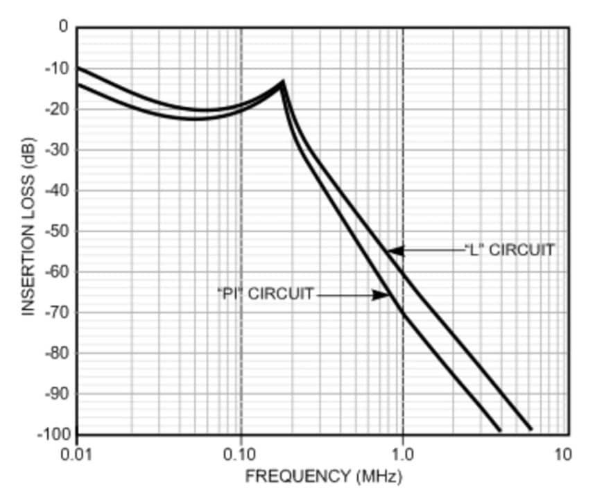
In this more realistic setting, 50 ohm source and 1 ohm load, the “L” circuit performs almost as well as the “PI” circuit as illustrated in Figure 5. By slightly increasing the values of C1 and L2 in the “L” circuit, a response identical to the “PI” circuit can be achieved.
In the above example we were only concerned with EMI emanating from the test sample. If we were also concerned about protecting against unwanted interference entering the device then a “T” circuit would be the filter of choice. In essence, by using a “T” circuit we have two “L” circuits with the inductor facing the lower impedance.
If the “T” circuit consisted of L1 facing the unit under test and, L3 facing the load with C2 in the middle, then for conduced emissions the “L” circuit is comprised of C2 and L3. For conducted susceptibility, if we assume the unit under test to be the lower of the two impedances, the “L” circuit is comprised of C2 and L1. In both instances the secondary inductor will provide some additional filtering. However, its contribution is relatively small compared to the other two components.
There are an infinite number of source and load impedance combinations for signal line applications where the 10 µfd line stabilization capacitors are not required as part of the test configuration. For these situations the theoretical insertion loss can be calculated by varying RS and RL in the equations.
Although the circuits that we have been discussing only address common mode (interference which is present as a common potential between ground and all power lines) EMI, the same philosophies apply when selecting differential mode (interference which is present as a potential between individual power lines) EMI filtering elements commonly found in multicircuit filter assemblies, or “Black Box”.
Conclusion
Selecting the proper EMI filter circuit is not a difficult task provided, that as a minimum, the following parameters are taken into consideration:
- The EMI source impedance
- The EMI load impedance
- The EMI propagation mode (common mode, differential mode or both)
- Conducted emission requirements
- Conducted susceptibility requirements
Other considerations that are not readily apparent are the effects caused by mismatching; performance at full load; and the inability to achieve the theoretical insertion loss due to the inductance (ESL) and resistance (ESR) in the capacitor, and the parasitic capacitance in the inductors.


