EMI filter performance plays a critical role in limiting emissions and also impacts the immunity of end-use equipment to electrical disturbances.
Philip F. Keebler and Kermit O. Phipps
EPRI, Knoxville, Tenn., USA
Today, electronic equipment is commonplace in every residential, commercial, and industrial environment. Moreover, this equipment depends on increasingly complex analog and digital circuitry and quality voltage input. These trends emphasize the necessity for conducted line emissions filters that perform well in unknown electrical environments. Manufacturers of end-user equipment do not rely on one standard type of filter. Instead, such equipment may include off the- shelf filters or custom designed ones. Regardless of the type used, filters must be reliable. Filter reliability is an important but multi-faceted concept. A reliable filter must limit the conducted emissions generated by the equipment, must maintain filter attenuation and insertion loss in normal electrical environments where overvoltages are sure to occur, and must provide a quality voltage to electronics downstream of the filter.
BRIEF OVERVIEW OF RADIO FREQUENCY (RF) LIGHTING CONDUCTED EMISSIONS STANDARDS: LIMIT LINES AND SAFETY MARGINS
In the end-use equipment industry, where a piece of equipment must be connected to the public power system or to another piece of equipment in the workaday environment, the level of conducted emissions must be controlled. In the United States, the Federal Communications Commission (FCC) issues limits that govern the level of emissions that can be injected into the AC line powering the equipment. For end-use devices, the FCC does not limit the level of emissions that can be injected onto control or other low-voltage cables attached to equipment. Thus, EMI filters are not required on the control circuits of end-use equipment marketed and used only in the United States. In the European Union (EU), the level of conducted emissions that can be injected into the AC line input is lower for every equipment category. These levels, issued and published by the International Electrotechnical Commission (IEC), include more stringent limits to prevent EMI problems with radio services or other electronic equipment. Not surprisingly, the EU limits the conducted emissions on the control circuits of end-use equipment marketed and used in the European market, and EMI conducted filters must be used on control circuits of this equipment.
Table 1 lists the levels of conducted emissions allowed by the FCC and the IEC for radio-frequency (RF) lighting devices that can be used in residential, commercial, and industrial environments. Table 1, clearly indicates that FCC and IEC requirements differ as to levels of emissions, the referenced frequency bands, types of equipment covered, and operating environments. Generally, RF lighting devices used in a residential environment are required to emit lower levels of emissions, and equipment used in commercial and industrial environments are permitted higher levels of emissions.
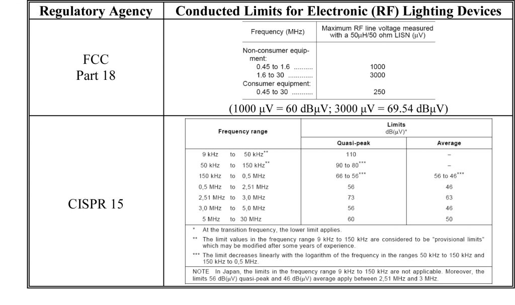
Obviously, the objective of designing and utilizing an EMI filter is to maintain the level of conducted emissions below the limit level promulgated by the respective regulatory agency. Still, some EMI filter designs simply do not provide enough margin in conducted emissions levels for end-use equipment to prevent the emissions from exceeding the prescribed limit. Neither Part 18 of the FCC nor CISPR 15, for example, specifies any specific tolerance (safety) margins for conducted emissions. Technically, this omission creates a kind of EMC “brinksmanship” with the filter designer and EMC test engineer determining just how close the conducted emissions level can come to exceeding the prescribed limit.

Figure 1 illustrates an example of conducted emissions measurements for Line 1 (hot conductor) of an electronic ballast operating at full load at 208 volts. In this example, the safety margin is 5.33 dBμV (60 – 54.67 dBμV). Although this margin will vary a few dB from sample to sample, it is not likely to become so small that the emissions cross the limit line. On the average, the emissions will be below the limit line. However, in actuality, the elements of an EMI filter age with time, equipment use, and exposure to electrical disturbances such as voltage surges. Then, the emissions will gradually increase with age and exposure to voltage surges and cross the limit line even when a metal oxide varistor (MOV) is used to protect the EMI filter. Electrical disturbances below the MOV’s clamping voltage will make it past the MOV and into the filter, degrading the performance of the X and Y capacitors and can affect the level of emissions anywhere along the frequency band.
BASIC AND ADVANCED EMI FILTER TOPOLOGIES
Like other electronic devices, electromagnetic interference (EMI) filters have evolved from very simple to very complex topologies. In filters, the simplicity or complexity of topologies is dependent on the need for flexibility in the desired attenuation performance and allowable equipment leakage current, which determines the required number of filter stages and elements. Using passive components, generally inductors and capacitors, it is impossible for one inductor and one capacitor to provide the desired level of attenuation across a wide frequency band. An EMI filter is designed so that its elements and stages work together to provide the necessary attenuation (or insertion loss) at various frequencies of interest for a particular frequency band. If the impedance of one or more elements is damaged by electrical disturbances, then the overall filter performance will begin to degrade sporadically, with the degradation being more severe in some frequency areas than in others. (A filter element is defined as a passive component such as a capacitor, inductor, or resistor that can dissipate electrical energy. A filter stage is defined as a group of filter elements that act together as a network to dissipate electrical energy at various levels depending on the magnitude and frequency of noise emissions currents.)
Table 2 illustrates some basic and advanced filter topologies. Typically, one-stage and two-stage filters are basic filters, while three-stage filters are designated as advanced filters. End-use equipment with a simple emissions signature and low levels of emissions can use basic filter topologies to maintain conducted emissions levels below the limits promulgated by the respective agency. Conversely, end-use equipment with complex emissions signatures with high levels of emissions and low leakage current limits must use advanced filters.

Table 2 shows that the complexity of EMI filters varies from filter to filter. One important observation is that an across-the-line capacitor (X capacitor) is not always the first element of the filter to be exposed to an electrical disturbance although, in most filter applications, the first element will be the X capacitor. The increasing complexity of EMI filters has tracked the complexity of end-use electronic equipment itself. A piece of equipment that contains a switching power supply and several types of digital circuits will require an EMI filter that is more complex (i.e., an advanced filter) than a piece of equipment containing a linear power supply and analog circuits, for example. Equipment that contains multiple switched mode power supplies and racks of processors will necessitate “heftier” filters. It is also common practice for large electronic systems to use filters in various stages of equipment.
In terms of system compatibility, EMI filters play one basic role—they are designed into equipment to limit the level of conducted emissions that are injected back onto the AC mains. As a result of their placement in the AC line circuitry, they play an important role in system compatibility vis-à-vis the quality of power on the AC line. EMI filters must be reliable and must perform as designed. Their performance must not be affected by the quality of power on the line. In addition, because of their location on the AC line, they must not create a poor power quality condition on their output. Designers of EMI filters and equipment should note that the voltage that appears on the output of an EMI filter is the voltage that is delivered to the working electronics of a piece of equipment. The working electronics generally starts with a bridge rectifier. If a voltage anomaly on the input to an EMI filter is further degraded by the filter itself, then the voltage delivered to the working electronics will be further degraded as well.
FILTER RELIABILITY AND PERFORMANCE AS A FUNCTION OF POWER QUALITY
The reliability and performance of EMI filters is critical to the operation of a piece of equipment. An EMI filter is almost always placed in the AC input line circuitry of the equipment. EMI filters are placed as close to the AC input line as possible to effect maximum reduction in the conducted noise emissions generated by the equipment before it is connected to the AC line.
A filter will also be subject to various levels of exposure to damage from incoming electrical disturbances depending upon the location of the filter in the AC input line circuitry. The types of disturbances that can damage an EMI filter are not limited to overvoltages such as voltage surges, voltage transients, temporary overvoltages, and voltage swells. Voltage distortion, voltage notching, and various types of undervoltages can also cause permanent damage to EMI filters. The effects of voltage surges, voltage transients, temporary overvoltages, and voltage distortion are used as examples in this article.

Figure 2 illustrates the typical location of an EMI filter in the AC line input circuitry for a piece of single-phase end-use equipment. One can see that the line fuse, overtemperature device (if one is used), and the MOV are typically situated before the EMI filter and not included in the filter. The Underwriters Laboratory (UL) requires that the line fuse appear in the AC line before the MOV to provide overcurrent protection for the equipment should the MOV become shorted. If the MOV shorts, then the line fuse will open up.
MOV PLACEMENT
Metal oxide varistors (MOVs) continue to play a critical role in protecting enduse equipment from voltage surges. Because the MOV and EMI filter must reside together in the AC line input circuitry with the MOV usually placed in front of the EMI filter, their combined performance and interaction also play a critical role in this protection. This protection not only involves the protection of the equipment from electrical disturbances but also the protection of the EMI filter from disturbances. Aside from the fuse and MOV, the EMI filter is the first system with passive electronic components to incur an overvoltage—a voltage transient or temporary overvoltage (TOV). An overvoltage that does not cause the MOV to conduct (clamping the disturbance) will pass right through the MOV, and its full energy content will enter into the EMI filter. Not all of the energy associated with an overvoltage can be dissipated by an MOV, and much of the energy that does pass through an MOV must be dissipated by the components within the EMI filter.
Unfortunately, not all equipment designers place MOVs in front of EMI filters. Some designers may place them on the output of an EMI filter. In such an application, the EMI filter is afforded no overvoltage protection by the MOV, and the EMI filter is far more susceptible to overvoltages.

INDUCTOR FLASHOVER
Like capacitors, inductors must be designed to withstand excessive amounts of electrical potential that may occur as the result of a transient or steady state voltage condition. In designing and rating inductors for use in EMI filters, most designers think of inductance, leakage inductance, and the current rating of the lead wire that is used to wind the inductor as the critical parameters. Inductor lead wire is different from other standard lead wire in that it is dipped in some type of solution (usually a specially designed varnish). The purpose of the varnish is to provide a dielectric that electrically isolates one winding from another so that a voltage may be established across the inductor.
However, voltage that is developed across the inductor (or throughout its windings) is not linear with the number of windings (or lead wire length). This non-linearity results in higher voltages being developed between windings that are closer to the inductor core. This non-linearity also results from higher values of magnetic flux that cross the windings closer to the core as compared to the last windings on the outside of the inductor. If these higher voltages are not taken into consideration when the type of varnish is chosen for the windings, then inductor flashover may occur as a result of dielectric (or varnish) failure. Varnish failure may also be accelerated by the occurrence of winding temperatures that are too high near the core. For example, when inductors are wound, this effect can become more predominant because of the mechanical stresses placed on the varnish coating. When inductor flashover occurs, the dielectric fails and part of the inductor’s windings become shorted, resulting in complete failure of the inductor. In addition, in some rare cases the inductor opens and the end-use equipment fails. With complete inductor failure, the EMI filter no longer provides a continuous path for current to flow, and the end-use equipment fails.
X AND Y CAPACITOR FAILURES
Capacitors play a major role in the design and operation of EMI filters. The impedance of a capacitor is inversely proportional to the frequency and the capacitance. For a fixed capacitance, the impedance of a capacitor decreases as frequency increases. This decrease in impedance continues until the self-resonant frequency of the capacitor is reached. At frequencies above this point, the impedance increases, and the capacitor approaches inductivity.
The EMI filter capacitors referred to as Class X capacitors are used in “across-the-line” applications where their failure would not lead to electric shock. These safety caps are used between the “live” conductors carrying the incoming AC current. In this position, a capacitor failure should not cause any electrical shock hazards. Instead, a capacitor failure “between-the-lines” would usually cause an overcurrent protective device to open. Thus, when an X cap fails because of overvoltage such as a surge or temporary overvoltage, it is likely to fail shorted. The failure of an X cap will cause an overcurrent condition and will cause the line fuse or circuit breaker to open.
The EMI filter capacitors referred to as Class Y capacitors are used in “line-to-ground” (line bypass) applications where their failure could lead to electric shock if a proper ground connection were lost. The failure of a “line-to-ground” capacitor would not cause the line fuse to open. In other words, the failure of a line bypass capacitor could create a 120-volt “hot” chassis that could result in a potentially fatal shock if the Y cap failed to open as designed.
For 120-volt rated end-use equipment, X and Y capacitors will have a steady-state voltage rating of 250 volts AC. This rating is acceptable for equipment used in the United States, Canada, Europe, Australia, and other countries where 230 or 240 volts are used. However, 250-volt rated X and Y capacitors should not be used for end-use equipment rated at 277 volts such as electronic lighting ballasts and adjustable speed drives. X and Y capacitors rated at 440 volts AC should be used for end-use equipment rated for 277 volts AC operation.
X- and Y-capacitors are referred to as safety capacitors in end-use and EMI filter design. These capacitors are grouped into several different classes. For the X-caps, there are three classes: X1, X2, and X3. For the Y-caps, there are four classes: Y1, Y2, Y3, and Y4. Most end-use equipment uses either X1 or X2 and Y2 capacitors. X1 capacitors are impulse tested to 4000 volts, X2 to 2500 volts, Y1 to 8000 volts, and Y2 to 5000 volts.
X2 and Y2 capacitors are the most popular and are typically found in appliances that plug into ordinary 120- volt receptacles. X1 and Y1 capacitors are used in heavy duty industrial enduser equipment such as an industrial computer or industrial electronic ballast that is connected to a three-phase line operating either at 208 or 277 volts AC.
X1 and Y1 capacitors cost more in EMI filter design and are larger in size because of their increased use of dielectric material to withstand the higher impulsive line voltages. Y capacitors must be more robust in withstanding higher line voltages because one leg is connected to ground. They are designed to fail safely by opening. Y capacitors are not used for X capacitor applications because Y capacitors are typically larger and cost more. Some capacitors have dual ratings such as X1/Y2, which means that they have met both X1 and Y2 safety requirements and standards.
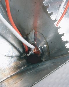
Figure 3 illustrates an example of a failed Y ceramic capacitor of the feed-through type. This capacitor was designed in between two filter stages to provide improved filtering over a traditional board-mounted Y capacitor. The burned marks at the bottom of the photograph indicate the failure.
The failure here was the breakdown that occurred between the line (center post of the capacitor, white wire) and the grounded shell of the capacitor as a result of a voltage surge. Two Y capacitors of the feed-through type are shown in Figure 3. The filter was improved by changing the soldering technique for attaching the wires to the posts of the feed-through capacitors.
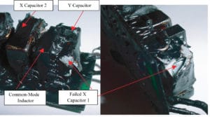
Figure 4 illustrates an example of a failed X capacitor inside an electronic fluorescent ballast. Clearly, the X capacitor on the line-side of the commonmode inductor failed. This capacitor was connected from line to neutral. The failure was due to an overvoltage (i.e., voltage surge). This ballast did not contain an MOV for surge protection.
X CAPACITOR: RESONANT FILTER EFFECTS FROM SURGES
X-caps are capacitors that are placed directly across the line voltage from one line to another line or to the neutral. X-caps are exposed to the line voltage at all times during the course of their filtering and are expected to survive without damage to their dielectric material. X-caps must be able to provide filtering in EMI filters when exposed to the line voltage. In other words, they must be able to withstand the line voltage environment.

However, the line voltage will not be the only voltage that the X cap undergoes. X caps must withstand any voltage that appears across the line—line-to-line voltages as in three-phase applications and line-to-neutral voltages for single-phase applications.
X capacitors may also be exposed to overvoltages caused by resonance effects. Such effects may be stimulated by voltage surges including ring and combination wave voltages. These surge voltages contain characteristic frequencies that can cause filter elements to resonate. Resonance effects among filter elements can result in incremental voltages developing across the elements .In some cases, it is even possible for these voltages to reach values that are higher than the voltage withstand limits of the X capacitors.
Figure 5 illustrates a case in which a filter (type C-L-CL- C using two common-mode inductors for the Ls) developed a resonance condition on the filter output. When a 1000-volt combination wave surge voltage was applied to the filter input, the result was a voltage on the filter output that was more than 1.6 times the input voltage. Such voltage magnifications are not uncommon in multi-stage filters and may contribute in damage to electronic components downstream of the filter. Equipment designers may choose to select inductors and capacitors for multi-stage filters in which resonant points do not overlap, or they may place an appropriately-sized MOV on the output of the filter to clamp magnified voltages.
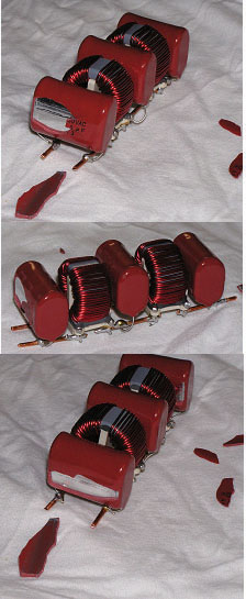
Figure 6 illustrates how a simple EMI filter can be damaged from a combination wave surge voltage. The photographs show that both the line-side and load-side X-capacitors were damaged. The line-side X-capacitor was subjected to a 1000-volt surge. That surge voltage was magnified by the filter and resulted in a larger voltage (1600 volts, see Figure 5) on the load-side X-capacitor.
CLEARANCES

In EMI filter design, the subject of electrical clearances is extremely important. Maintaining proper clearances between solder pads, elements leads, element bodies, and grounded surfaces will help avoid breakdown within the EMI filter. Dielectric breakdown may occur between any two surfaces or edges. One may design component spacing and arrangement of filter elements so that breakdown does not occur at maximum line voltage (e.g., 305 volts AC for a 277-volt system) or a voltage prescribed by a safety-related test such as a hi-pot test. However, one may suddenly discover that dielectric breakdown may occur during surge testing at surge test voltages that are less than the clamping voltage of an MOV. Breakdown at these voltages should also be avoided to prevent permanent damage to an EMI filter during voltage surge conditions that are not severe enough to activate an MOV. Dielectric breakdown may be avoided by using substances with high dielectric permittivity such as specialized potting materials. Figure 7 illustrates an example of a dielectric breakdown that occurred as a result of improper clearances between the printed-circuit board and the shielded enclosure of the EMI filter.
EQUIPMENT SUSCEPTIBILITY AS A FUNCTION OF FILTER DESIGN
Inductor Saturation
Common- and differential-mode inductors are used in EMI filters to provide inductive impedance within specific frequency bands. The line current that must pass through the filter must also pass through the inductors. The amount of load current that must pass through an inductor affects the ability of the inductor to provide inductive impedance. If a load current is too high, then an inductor may begin to saturate. Saturated inductors critically affect the performance of the filter operation below the frequency of 100 kHz.
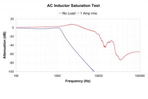
An inductor of an EMI filter may be operating near or in saturation during steady-state operation of the end-use equipment. In this case, the attenuation performance of the filter suffers throughout equipment use until the load current is reduced allowing the inductor to operate without saturation. In other instances, an inductor may temporarily operate in saturation when the load current fluctuates to the point where saturation is reached. Inductor saturation here can occur during the recovery of a voltage sag or momentary interruption condition when the line voltage begins to recover, thus causing a temporary increase in load current that forces the inductor into saturation.
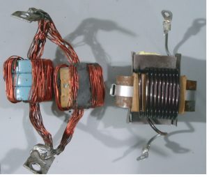
Figure 8 illustrates a power-line filter whose attenuation performance is affected by only one amp of load current flowing through the inductor winding. This inductor suffers severe attenuation degradation at frequencies greater than about 1 kHz.
Figure 9 illustrates two inductors both from powerline filters that may be used in facility shielded rooms or magnetic resonance imaging (MRI) shielded rooms. The inductor on the left saturates at a low (1-amp) filter load current. This inductor is made with a powdered core. The inductor on the right does not saturate up to a level of about 60 amps. It is made of laminate steel and is a cut C-core just the opposite of what one might expect.
WITHSTANDING TOVS AND CAPACITOR VOLTAGE RATINGS
Temporary overvoltages (TOVs) can go as high as 2.0 p.u. (per unit) voltages. In a 277-volt AC system, 2.0 p.u. equates to 554 volts RMS or 783.4 volts peak. For X capacitors rated at 440 volts AC for 277-volt systems, a 2.0-p.u. TOV will exceed this rating. Over time, subsequent TOVs at these voltages will degrade the dielectric material in the X capacitors. Thus, the equipment designer may want to select an MOV with a clamping voltage that will help to reduce the exposure of an X capacitor to TOVs, and/or select a higher rated capacitor.

CAPACITOR SWITCHING EVENTS
The capacitor switching-based ring wave, defined in ANSI/ IEEE C62.41.2-2002, IEEE Recommended Practice on Characterization of Surges in Low-Voltage (1000 V and Less) AC Power Circuits, occurs largely because of the switching of capacitor banks. The waves can deposit high energy into electronic devices including electronic lamp-ballast systems because of their long duration. Traditionally, the peak surge-voltage value defined in ANSI/IEEE C62.41.2 is 1.8 times (1.8 p.u.) rated Vpeak for the high-exposure environment, 1.0 times rated Vpeak for the medium-exposure environment, and no test is recommended for the low-exposure environment. Thus, the highest total peak surge voltage that could be used in this test (if applicable), including the mains voltage, is 2.8 times Vpeak. The capacitor-switching test should be considered when the ballast is exposed in an environment near large switching-capacitor banks. In this test, the peak surge voltage is selected to be no greater than 2.0 times rated Vpeak, which is the general specification for this test as prescribed in ANSI/IEEE C62.41.2-2002.
The frequencies at which capacitor events can occur ranges from a few hundred hertz to several kilohertz that may excite EMI filters designed with X large capacitor values (e.g., greater than 0.047 μF). Resulting resonance can create damaging and magnified voltages across the filter elements as previously discussed. A secondary effect, which affects end-use equipment operation, is the resulting rise in DC bus voltage as seen in Figure 10. This 56-volt rise shown on the DC bus may easily cause equipment to trip on overvoltage conditions.
DISTORTED AND FLAT-TOPPED FILTER OUTPUT VOLTAGES
Each element in an EMI filter will drop voltage at low frequencies (e.g., 60 hertz up to several harmonics) and at high frequencies where emissions filtering must occur. In filter design, the voltage drop at low frequencies should be minimal. However, system compatibility research ar EPRI has shown that capacitive and inductive elements in EMI filters can cause significant distortion and can “flat-top” the 60-hertz sine wave voltage that appears at the filter output.
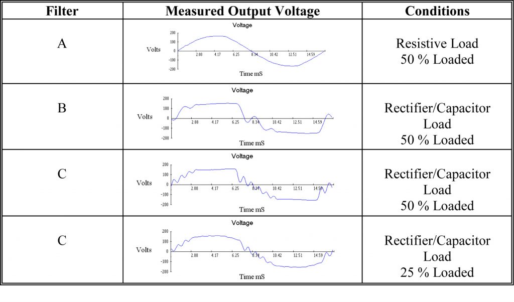
Table 4 illustrates four examples of the effects of linear and non-linear loading on three different EMI filters with loads not exceeding their current rating. Filter A illustrates that it is possible to obtain a sine wave type output voltage with low distortion using a resistive load on the filter output. Filter B illustrates how severe distortion and flattopping can occur when a filter is loaded with a non-linear (rectifier/capacitor) load similar to those found in electronic end-use equipment. Filter C illustrates the same type of voltage quality problem at the filter’s output when a nonlinear load is applied and that the degree of distortion in the output voltage is related to the degree to which the filter is loaded. Filters B and C in this example are filters that used inductance values that were too high and capacitance values that were too low. Selecting the appropriate mix between inductance and capacitance will help to avoid this type of distortion and flat-topping on the output voltage. Some filter capacitances can be increased within reason until filter leakage current specifications are met. If lowering inductance values and increasing capacitance values will not provide the necessary amount of attenuation, then additional filter stages should be considered in the filter design. When designing or selecting an EMI filter for end-use equipment, the designer should check the quality of the filter output voltage under all equipment-loading conditions. This step is a vital safeguard that must precede finalizing the filter design. Distorted and flat-topped voltages on the output of a filter effectively lower the RMS value of the voltage; thus making the equipment more susceptible to disturbance such as voltage sags and momentary interruptions.
CONCLUSION
The quality of voltage delivered to end-use equipment includes electrical and electromagnetic disturbances that occur at low frequencies (e.g., 60 hertz) and at high frequencies (e.g., greater than 1 kHz). The performance of EMI filters plays a critical role in limiting emissions and also impacts the immunity of end-use equipment to disturbances. EMI filter designers who do not investigate the reliability of filter elements or the effects of the voltage quality at the output of a filter may very well find themselves analyzing equipment and/or filter failures and re-working their designs.
BIBLIOGRAPHY
[1] ANSI/IEEE 1560, American National Standard – IEEE Standard for Methods of Measurement of Radio-Frequency Power-Line Interference Filter in the Range from 100 Hz to 100 kHz (2005).
[2] ANSI C62.41.2, American National Standard – IEEE Recommended Practice on Characterization of Surges in Low-Voltage (1000 V and Less) AC Power Circuits. (2003).
[3] Carter, Mark. “AC Capacitors and Power Quality.” Powertechnics Magazine. March 1990.
[4] CISPR 15, Limits and methods of measurement of radio disturbance characteristics of electrical lighting and similar equipment. (2002).
[5] Federal Communications Commission (FCC) Part 18 – Industrial, Scientific, and Medical Equipment, 47 CFR, Chapter 1 (1998).
[6] Keebler, Philip F., Phipps, Kermit O, and Nastasi, Doni. “Distinguishing Between Surge- and Temporary Overvoltage-Related Failures of Metal Oxide Varistors in End-Use Equipment Designs.” Interference Technology EMC Directory & Design Guide, 2005.
[7] Phipps, Kermit O., and Connatser, Bradford R., “Understanding MOVs for Applying Robust Protection Against Surges.” Interference Technology EMC Directory & Design Guide, 2005.
ABOUT THE AUTHOR
Philip F. Keebler has conducted System Compatibility Research on personal computers, lighting, medical equipment, and Internet data center equipment. The lighting tasks were associated with characterizing electronic fluorescent and magnetic HID ballasts, electronic fluorescent and HID ballast interference, electronic fluorescent and HID ballasts failures, electronic fluorescent and HID lamp failures. He has drafted test protocols and performance criteria for SCRP tasks relating to PQ and EMC. Mr. Keebler also manages the Electromagnetic Compatibility (EMC) Group at EPRI where EMC site surveys are conducted, end-use devices are tested for EMC, EMC audits are conducted, and solutions to electromagnetic interference (EMI) problems are identified. He has completed his service as editor developing a new EMC standard for power-line filters, IEEE 1560.
Kermit O. Phipps is a NARTE Certified EMC engineer and conducts tests and evaluations of equipment performance in accordance with standards of ANSI/IEEE, IEC, U.S. Military, and UL, as well as with the EPRI System Compatibility Test Protocols for EPRI. He served in the U.S. Air Force as a manual electronic warfare and component specialist, resolving hardware and software problems. He conducts research on surge protection, power-line filters, shielding effectiveness, and electromagnetic interference. Mr. Phipps is the author and co-author of test plans, protocols, and research papers presented at international power quality and EMC conferences. He has conducted a number of power quality and EMC training sessions and field investigations. Most recently, he has completed his voluntary work as chairman in developing anew EMC standard for power-line filters, IEEE 1560.


