INTRODUCTION
IN THE SEMICONDUCTOR SECTOR TODAY, ESD sensitive devices can be damaged at <+/-50 volts. Aerospace & Defense cannot issue a Return Materials Authorization (RMA) for an ESD sensitive device that fails in space or a nonfunctioning weapon system in-theatre. The fact that extruded film can charge up to over +/- 100,000 volts below 20% RHhas been problematic for polymer and paperboard manufacturers for years. The Santa AnaWinds of Southern California and winter conditions of Colorado can produce relative humidity (RH) levels at <4% RH. Shortly after takeoff, the RH can drop from 60% on the tarmac to <9% in the cabin after 20 minutes in flight1. In the pharmaceutical industry, microprocessor driven liquid crystal display scales can freeze up due to electrostatic discharge in proximity of Teflon conveyor systems. However,this magnitude of scale for Triboelectrification or charge generation may not be an issue for many areas of the semiconductor sector.
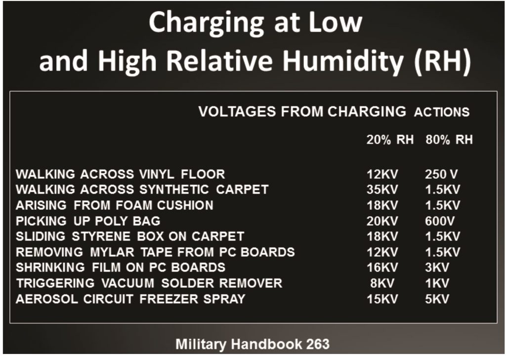
Table 1 – A well-known charge relationship between charging
and RH levels is illustrated in Table 1.
The Aerospace & Defense sector has many areas in which charge generators can not only damage ESD sensitive devices but can also pose issues with personnel due to shock. The author has personally been involved with large electrostatic fields produced from antistatic pink poly pallet bags, taping operations, conveyorized charge generation issues and satellite shroud charging. Consequently, in some cases, a distance of one meter may not be far enough for charge generators listed in Table 2. Traditionally, in the EPA, 30% to 70% RH has been targeted as an ESD control measure. One excellent source for traceability is the Workmanship NASA-STD 8739.6, Section 6.1.
6.1 TEMPERATURE AND RELATIVE HUMIDITY (RH)
6.1.1 Temperature and relative humidity (RH) shall be monitored in the processing area and maintained within the following limits (Requirement):
a. For temperature: 18° – 30° C (65° – 85° F)
b. Maximum relative humidity: 70 percent RH
c. For ESD-sensitive hardware, minimum humidity: 30% RH
d. For ESD-sensitive hardware, HBM Class 0, minimum
humidity: 40% RH
6.1.2 For instances where maintaining an RH level shown in c. or d. above is not practical, special methods, procedures, equipment, and assurance requirements designed to overcome the risks of relative humidity levels below 30% RH shall be used and documented in the applicable ESD Control Program Plan. If an electrostatic field is in proximity to ESD sensitive devices, then a Field Induced Model (FIM) discharge can take place. Section 8.3.1 on Insulators of ANSI/ESD S20.20-2014 states: “If the field measured on the process required insulator is greater than 2000 volts/inch and the process required insulator is less than 30 cm (12 inches) from the ESDS item, steps shall be taken to either:
A) Separate the required insulator from the ESDS item by a distance of greater than 30 cm
B) (12 inches); or
B) Use ionization or other charge mitigating techniques to
neutralize the charge.”
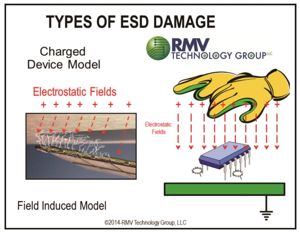
Figure 1

Table 2
The 1 foot rule is inadequate for insulators that can produce far greater voltages than 2000 volts/inch at a distance greater than 1 meter (3.28 feet). At moderate and low RH conditions, large charge generating insulators can still pose problems with ESD sensitive devices.ANSI/ESD S20.20 states: “If the field measured on the process required insulator is greater than 125 volts/inch and the process required insulator is less than 2.5 cm (1 inch) from the ESDS item, steps A and B above shall be taken. It should be noted that several end user organizations inside and outside the aerospace & defensesector set a limit of <+/-100 volts for ultrasensitive ESD devices.
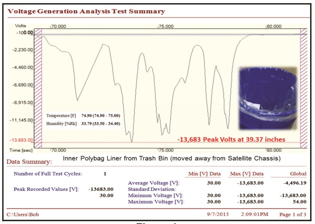
Figure 1
In the first example, a blue polymer trash bin was incorrectly positioned approximately
6 inches from an ANSI/ESD S4.1 safe satellite chassis. The resting voltage measured -4,490 volts/inch from the polymer bag trash bin liner. When the trash receptacle was moved away from the satellite, voltage measured -13,683 peak volts at 1 meter when the clear polybag liner was removed from the blue plastic container. Note: The operator was grounded during the measurement process (satellite is not pictured). Moving approximately 1 foot away from the solar panel array produced voltages of 20,400 and -5,011 volts (Figure 2). To simulate charge generators at 1.0 foot, the laboratory environment was preconditioned to 30% RH at 730F +/-50F for48 hours. In facilitating this test, the insulative polystyrene sheet was grounded. The sheet was simply lifted from a set of several sheets to enable charge-separation (friction) or contact separation. The polystyrene sheet was positioned 1 foot from a non-contact voltage meter and measured -12,440 volts (Figure 3). Clearly, the voltage from insulators can pose a risk to ESD sensitive devices if the >1 meter rule is not enforced within an aerospace EPA. In Figure 4, the antistatic film peaked out the measuring range of the electrostatic field meter (>20,400 volts) because the topical antistat was inadequate to minimize charge bleed-off. It has been estimated that antistat accelerated agingtesting takes approximately 12-14 days2. One day at 1600F equals 17 days at room temperature. Thus, a topically coated antistatic sheet may losethe ability to prevent triboelectrification in 204 to 289 days (more or less).
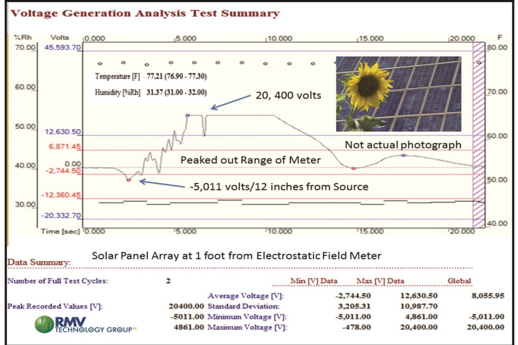
Figure 2
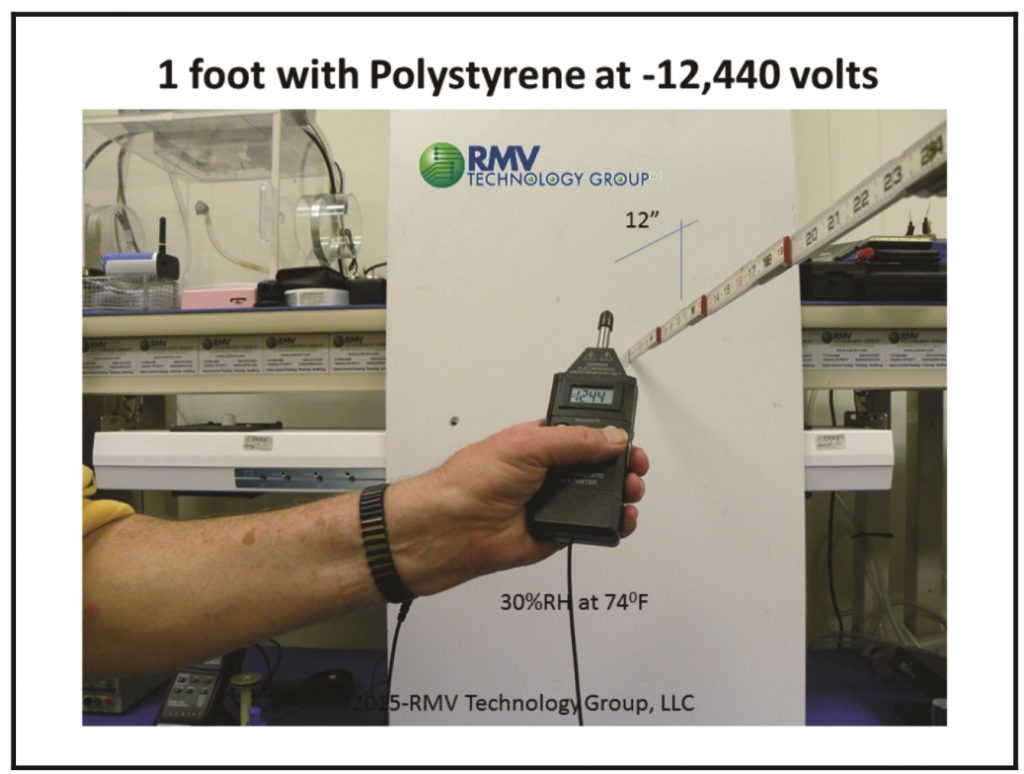
Figure 3
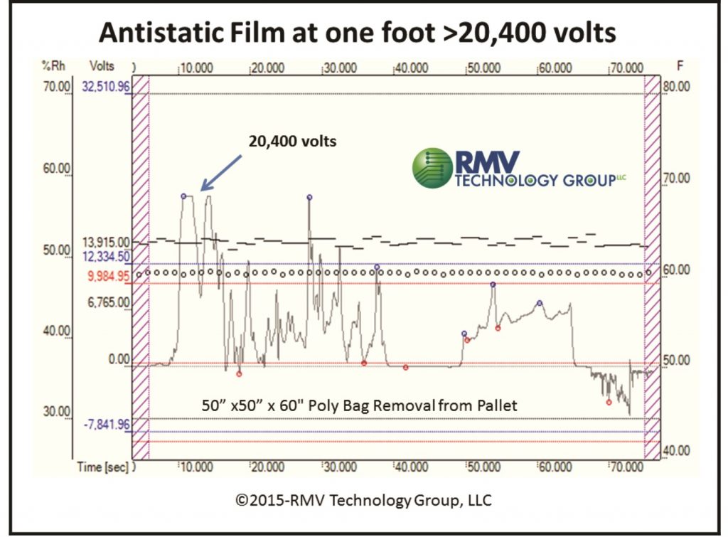
Figure 4
Antistats for long term storage pose issues with longevity and humidity performance during transport and storage. Accordingto the late John Kolyer, Ph.D. (Boeing, retired), antistats can lose effectiveness at 9% RH. Non-treated Lexan polycarbonate can pose a problem with charging. Product moved along a conveyorized system about 18 inches from the charge source. The inside of the Lexan enclosed environment measured 20%RH, 800F; the outside environment measured 50% RH, 600F. When the Lexan door was opened by a technician (Figure 5), the rapid rush of air against the polycarbonate door generated 147,400 volts at a distance of 6” using a special static locator capable of measuring between +/-100 volts to +/-200,000 volts. Damage to the product had taken place. At a distance of 18 inches, two ionizers were in operation. The voltage seen on the conveyorized pallet due to the charge generating Lexan door (Figure 6) produced a reading of 6,010 volts. Treatment of the door’s surfaces with an inherently conductive polymer film was utilized while grounding the Lexan door to mitigate charging. In Figure 8, the reader can see that removal of 4 flat panel display sheets from a storage and transport mechanism accounted for large electrostatic fields at a moderate 39.5% RH level. It should also be noted that transport-storage mechanisms for flat panels (type used in Figure 7) were not grounded as the locking wheels and tile flooring were both insulative. In summary, one can see from Table 4 that larger insulative platforms require greater distances in excess of 1 foot, and, in some cases, more than one meter to minimize the effects of electrostatic field generation. A future article mapping Field Induced Model (FIM) discharge would be beneficial to demonstrate the relationship between charge generation and ESD events. If there are mission critical ESD sensitive devices, then one needs to adhere to the 1 meter rule as referenced in the NASA-HANDBOOK 8739.21.
REFERENCES
[1] The Dip Tube, Interference Technology, 6 May 2010, Vermillion,
Pages 72-80
[2] Mil-PRF-81705E
Mil Handbook 263B-1994
NASA-STD 8739.6
NASA-HANDBOOK 8739.21
ANSI/ESD S20.20-2014
ESDA Adv. 11.2-1995
Dr. John M. Kolyer, Ph.D., Rockwell International, Telephone interview
in 2004
The Charged Device Model & Work Surface Selection, John Kolyer and
Donald Watson, October 1991, pp. 110-117
Humidity & Temperature Effects on Surface Resistivity, John Kolyer and
Ronald Rushworth, Evaluation Engineering, October 1990, pp. 106-110
Triboelectric Testing at KSC Under Low Pressure and Temperature
ESD Association Proceedings 2002, Dr. Ray Gompf, PE
ABOUT THE AUTHOR
Bob Vermillion, CPP/Fellow, is a Certified ESD & Product SafetyEngineer-iNARTE with practical and “hands-on” expertise in the mitigation of material Triboelectrification on a Mars surface and in troubleshooting robotics or systems in aerospace, disk drive, medical device , pharmaceutical, automotive and semiconductor sectors. A co-author of several ANSI level ESD documents, Bob is a member of the ESD Association Standards Committee and conducts ESD Seminars in the USA and abroad, including guest speaker engagements for California State Polytechnic University, San
Jose State University, University of California at Berkeley, Lawrence Berkeley National Laboratory and Clemson University. In 2015, Bob has been invited to conduct a seminar at Oxford University. Bob is Chief Technology Officer of RMV Technology Group, LLC, a 3rd Party ESD Materials Testing, Training and Consulting Company. Bob can be reached at 650-964-4792 or bob@esdrmv.com
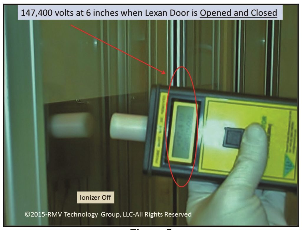
Figure 5
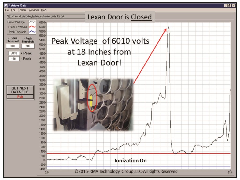
Figure 6
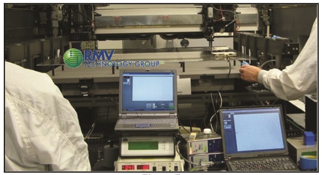
Figure 7
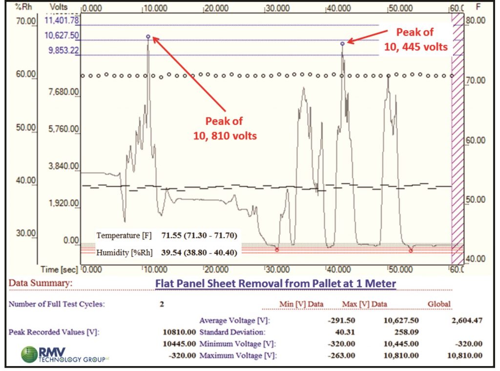
Figure 8
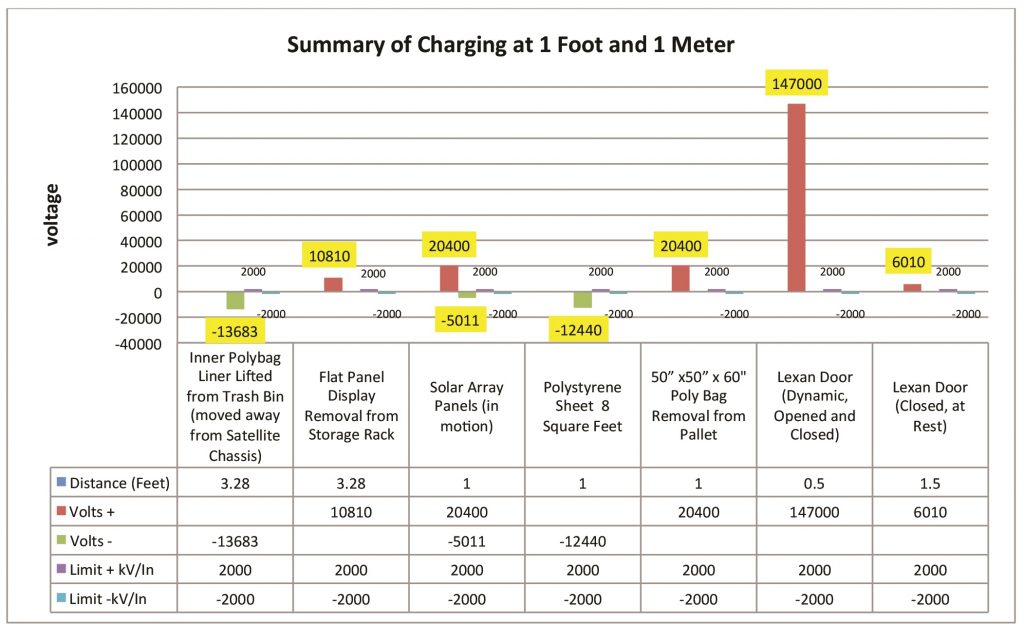
Table 4


