What is an EMC Design Review?
Most hardware engineers are used to doing functional design reviews on their circuit boards and systems before pressing the ‘go’ button for manufacturing. In the engineering teams I’ve worked with, that type of design review has usually taken the form of standing around a board room table with a red pen and the largest print outs of the schematics that we could get our hands on. It can also be done by just one person at a PC with cross probing enabled between schematics and layout (if your boss was kind enough to get that license!). We sifted through the design, pin by pin and connector by connector, determined to find an accidentally reversed interface or incorrectly pinned out symbol. You knew that there was a good chance that the schematics in front of you contained a hidden mistake that had the potential to turn your high end circuit board into an expensive beer coaster, or cost you a lot of rework time at the least!
Companies that are on the ball have standardized this kind of review process into a checklist based procedure that is run through and verified on each and every design. By doing this, they increase the robustness of the review and minimize the chances of a major issue slipping through the cracks.
Surprisingly, very few companies that I’ve been involved with over the years have migrated this important process into the EMC world. In just the same way that a functional design review can catch many design errors, a solid EMC design review can catch lots of known poor design practices for emissions and immunity performance. It can mean the difference between your product passing or failing at an EMC test lab.
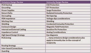
A good EMC design review should cover many aspects of an overall product design. At the top level, a design review should cover topics such as:
EMC as a Functional Specification
I like to think of EMC testing as a completely separate functional specification. There are a specific set of pass/fail criteria that your product must meet, or you can’t sell it. It’s that simple. Without a clear specification of the tests your product is going to be subjected to at an EMC lab, you are lacking a functional specification that should really be taken into account at the design stage of your project. You wouldn’t dream of designing a product without a clear view of the feature set being provided to the end customer would you? EMC testing is a just a different kind of feature set that your design needs to include. Without an EMC functional specification, you’re leaving a pass or fail at an EMC lab up to chance. Is it any coincidence then, that according to Intertek (one of the largest lab groups in the world), the global EMC first time pass rate is only 50%?
In this post I’m going to give an overview of what an EMC design review is and how to go about doing one on your next product.
Why Bother to do an EMC Design Review?
An EMC failure can very easily cost your company several thousand dollars in tangible expenses such as hiring a consultant, renting debug equipment, re-working/manufacturing designs and paying for re-tests. A larger concern for many companies is the delay to market that an EMC failure can cause. Since EMC approval is required before you can legally sell your product, a failure can introduce a delay to market of several days to several weeks. The longest delay to market that I’ve come across due to an EMC failure is about 4 months as the company really struggled to solve the issues through several design iterations, but I wouldn’t be surprised if longer delays exist.
Accountants generally agree that a delay to market will reduce the peak sales volume of any given product by a few percent and depending on the nature of your product, may reduce the length of the overall sales window. For many medium to large hardware companies, a 1 month delay can easily lead to a reduction in overall revenue for a particular product during its’ lifespan of greater than $1 million. Suddenly, considering EMC early in the design cycle doesn’t look like a bad idea at all.
Lastly, doing a robust EMC design review can increase the performance of your product and therefore reduce the number of customer returns. For example, a company that has a product with relatively poor immunity protection may get lots of returns due to damage from static discharges coming from the end user’s fingers when they’re pushing buttons on the product. Or perhaps the product will be used in a relatively noisy electromagnetic environment and the functioning of the device is affected in some ways such as degradation of RF performance or measurement accuracy. Good EMC design can reduce these sorts of issues.
Companies who are lucky enough to have an EMC expert on staff may not have implemented a robust EMC design review (yet), but the knowledge locked away in the expert’s head is probably already introducing an ad hoc review of sorts. What I’ve noticed is that design engineers who have significant experience with EMC testing tend to use their memory of EMC failure modes to avoid running into the same issues again in the future. For example, as they’re laying out a circuit board (or directing a draftsman), they may remember a time when a previous product they designed failed radiated emissions due to excessive noise on the external cabling. The engineer then takes whatever design improvement they implemented to reduce the noise on the cabling and applies that methodology to all designs in the future. What they’ve essentially done is to build up a set of design rules that they follow for each successive design. As they experience more EMC issues and solve them, they add these rules to their existing mental list.
Standardizing these rules into formal design review procedure is key to repeatedly performing a robust EMC design review. Companies such as Ford and Jaguar who face some of the toughest EMC challenges (automotive) implement robust EMC design reviews. I believe everyone can benefit from taking this approach. One huge benefit of a formalized EMC design review is that it can be undertaken by a relatively junior engineer without much experience in design for EMC compliance. This is because it’s much easier to check that a specific design rule has been implemented correctly than it is to do comprehensive EMC training and understand why a rule makes sense from a physics perspective. For companies without a seasoned EMC pro on staff, an EMC design review is a great way to quickly verify that your design has the best chance of passing EMC testing.
Unfortunately, most companies do not have a skilled EMC engineer on staff and do not have the in house knowledge to create an EMC design review process. EMC training is usually incredibly expensive, with typical pricing for a short 2-3 day seminar of >$1500 USD plus expenses per engineer.
I can’t go into every single item covered in a comprehensive EMC design review, but in this post I’m going to detail a few of the most important aspects that I always check. The section below gives you a top level overview of how I do EMC design reviews for clients.
How to Get Started
Define your Pass/Fail Specifications
Without a clear definition of the pass/fail criteria, you don’t have a good specification to work with. In some cases, your product may only be tested for radiated and conducted emissions performance. In others, your product may also be subjected to immunity phenomena such as ESD, surge and EFT. The first task is to detail the limits and levels for emissions and immunity that your product must achieve during EMC testing.
Emissions Limits
First, you should define what the emission limits are for your product. These may vary depending on the environment that your product will be used in and the regions of the world where it will be sold. One of the most important places to start is to work out whether your product falls under “Class A” or “Class B” limits. Here’s how the FCC makes the distinction:
Class A digital device: A digital device that is marketed for use in a commercial, industrial or business environment, exclusive of a device which is marketed for use by the general public or is intended to be used in the home.
Class B digital device: A digital device that is marketed for use in a residential environment notwithstanding use in commercial, business and industrial environments. Examples of such devices include, but are not limited to, personal computers, calculators, and similar electronic devices that are marketed for use by the general public.
It’s important to note that Class B limits are significantly lower than Class A limits.
Limits also differ between geographic region and between product types. Check the standards that apply to your product (or ask a test lab) to work out the limits that you’re going to need to meet.
I’ve included an example below of some limits for a class B unintentional emitting device so that you can see what it looks like. The lower and upper frequencies covered by the limits vary depending on the internal clock frequencies present within your product and also vary depending on the standards that apply to your product.
Although you can get a feel for the radiated emissions from particular nets in your design using free tools like the ‘Maximum Emission Calculator‘ tool from Clemson university, it isn’t very practical to use tools like this for analyzing a full design. Emission limits typically cover radiated and conducted emissions as well as Ethernet conducted emissions (if applicable).
Finding out the emission limits that apply to your particular product gives you a good idea of how difficult it’s going to be to get your product’s emissions below the limits.
Immunity Levels and Pass/Fail Criteria
If immunity testing applies to your product (usually mandatory for CE Mark and global product family standards), then it’s worth finding out what test levels an EMC lab is going to use, where the tests will be applied and how well your product needs to perform during and after the test (this is called performance criteria). This will help you to work out where to apply EMC suppression devices, what ratings to choose and will also give you an idea of how much care you need to take. If you have a regular test lab that you use, they should be happy to provide you with a test plan up front so that you can use it in the design stage of your product development cycle. If you have a relationship with a test lab, they should be willing to help you. If they’re not, it might be time to start looking for a different test lab.
You can see an example of an immunity test plan below, which includes the levels that will be applied to your product and the criteria that your product needs to meet.
The definition of the pass/fail criteria can vary a bit from standard to standard, but here is a description of each performance criteria taken from the international generic immunity standard for residential, commercial and light-industrial environments (IEC 61000-6-1):
a) Performance criterion A: The apparatus shall continue to operate as intended during and after the test. No degradation of performance or loss of function is allowed below a performance level specified by the manufacturer, when the apparatus is used as intended. The performance level may be replaced by a permissible loss of performance. If the minimum performance level or the permissible performance loss is not specified by the manufacturer, either of these may be derived from the product description and documentation and what the user may reasonably expect from the apparatus if used as intended.
b) Performance criterion B: The apparatus shall continue to operate as intended after the test. No degradation of performance or loss of function is allowed below a performance level specified by the manufacturer, when the apparatus is used as intended. The performance level may be replaced by a permissible loss of performance. During the test, degradation of performance is however allowed. No change of actual operating state or stored data is allowed. If the minimum performance level or the permissible performance loss is not specified by the manufacturer, either of these may be derived from the product description and documentation and what the user may reasonably expect from the apparatus if used as intended.
c) Performance criterion C: Temporary loss of function is allowed, provided the function is self-recoverable or can be restored by the operation of the controls.
It’s essential to find out the performance criteria that your product will have to meet at a test lab.
Emissions
1. Pick the right stack-up
Configuring the right PCB stack is fundamental to EMC performance. Without an adequate layer count for a given complexity and without the correct layer order and usage, you’re going to make your job of controlling radiated and conducted emissions pretty hard. If your boss is pushing you to reduce the layer count to save on PCB costs, just remember that there is usually a trade off with EMC performance, which has the potential to hurt the company wallet even more.
The desirable features of a good PCB stack (from an EMC perspective) are:
• Signal layers adjacent to plane layers
• Signal layers tightly coupled to return power/ground plane
• Power and grounds closely coupled
• High speed signals on buried layers
• Symmetrical
With those features in mind, here are sample layer stacks for 4 and 6 layer boards:
4 Layer Example Stack
In this diagram you can see a couple of different ways that 4 layer stacks can be implemented. See if you can work out from the desirable characteristics listed above, what the trade offs are for each stack.
6 Layer Example Stack
Can you work out why the stack on the left is not recommended?
I don’t have time to cover it here, but the stack geometry and PCB materials can also heavily affect EMC performance. That’s because it will define the impedance of nets and planes which can vary from layer to layer. Without careful consideration of the board impedance, you can run in to significant signal integrity and power delivery network (PDN) problems.
2. Does every IC have adequate de-coupling?
This one is repeated a lot, but it’s worth verifying and confirming during an EMC design review that every single IC has adequate decoupling. When I do EMC design reviews for clients, I usually find at least a couple of ICs or PWR/GND pin pairs where the designer forgot to add de-coupling caps or the caps have been implemented in a way that would make them pretty ineffective. You can see the effect of adding de-coupling to an IC below (reproduced with permission from Williamson Labs).
The upper left diagram shows the effect of de-coupling on supply noise in the frequency domain and the upper right diagram shows the effect in the time domain. You can see that the optimal performance is when the decoupling cap is place below the IC and routed as directly as possible between the PWR and GND pin pair.
It’s worth noting that the important characteristics of decoupling capacitors include not only the value of the capacitor (nF, pF etc) but also ESR (Equivalent Series Resistance) and ESL (Equivalent Series Inductance). This EDN blog post does a good job of explaining the effect of those characteristics on PDN impedance.
3. Check for breaks in the return path
If you’re not familiar with return paths, it just means the route current flows back to the source. Whenever you have an IC that supplies current to another device, there is an equal and opposite current that travels back to the source device.
The diagram above illustrates that the return path in DC travels the path of least resistance. The return path in AC (higher frequency signals) travels the path of least inductance, which is usually on a reference plane directly underneath the source signal. Whenever there is a cut in the return path on the reference plane, the return current has to flow around the cut to find the path of least inductance. This forms a nice current loop that has the potential to become an efficient radiator.
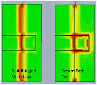
The diagram below shows a 0.5 GHz signal that traverses a cut in the ground plane. You can see in the right hand picture that the current distribution on the return path finds a way around the slot and therefore makes a loop. The left hand picture shows a scenario where the cuts in the return path have been bridged by capacitors which allow the high frequency return current to ‘jump’ over the gaps.
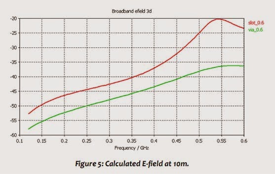
The effect on far field radiated emissions from this one signal might surprise you. The simulation of this scenario shows that emissions measured at 10 metres from this net alone can be more than 30 dB higher with a cut in the return plane. This can definitely mean the difference between a pass or fail at an EMC lab.
[Source unknown]
During an EMC design review, you should view your layout 2 layers at a time and carefully verify that all of your digital signals have a well defined return paths without cuts. If a cut in the return path is necessary for any reason, then ensure that the cuts have been bridged with capacitors that have low impedance at the frequencies of interest.
Immunity
1. Has ESD protection been applied to all external ports?
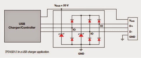
Once you know which ports of your product will be tested, you can add the ports to your EMC design review checklist. Now go and verify that each of the ports has adequate ESD protection on the circuit board, in the right places and of the correct rating. Here is an example of a USB port that has good ESD protection (from Texas Instruments).
Note that the protection should be placed as physically close to the port connector as possible. Many different types of ESD protection devices are available. Check out the ESD section in the “Getting EMC Design Right First Time” eBook for more details.
Closely related to this item is to verify that net to net clearances and and net to plane clearances near the ESD injection points do not allow for ‘arcing’. This is to ensure that the ESD can’t jump to another conductor and potentially cause damage elsewhere in the product. The suggested clearances required to ensure that arcs do not occur for given voltage levels in various circumstances are covered in the IPC-2221 standard.
2. Sensitive Circuitry Shielding
Radiated immunity is a very common test that applies to most electronic devices destined for Europe, or those that adhere to international product standards. The field strengths that your product may be subjected to can vary between 1V/m and 200 V/m depending on the standard. The field is also usually swept across the frequency range 80 MHz – 4 GHz (some standards may go higher and lower than this).
If your product contains sensitive circuitry such as analog measurement circuits or RF circuitry, then even low power radiated electric fields can introduce major issues. A common and inexpensive way to protect circuitry from radiated fields is to provide a small shield over the circuitry of interest.
A few simple checks that I do during an EMC design review are:
• Are there any circuit elements that are likely to be susceptible to radiated electric fields?
• Is shield grounded at multiple points?
• Is shield fitted tightly to PCB?
• Check solder joints are not dry
• Are apertures (e.g. for ventilation) in the shield minimized?
• If apertures are required, are they positioned at furthest point away from sensitive circuitry?
Note that shielding alone often isn’t enough to immunize your sensitive circuitry from radiated electric fields. Often the field is picked up by external cabling and is coupled on to a circuit board. Once that energy is on the circuit board, it can affect the sensitive circuitry by things like voltage fluctuations on the ground or power planes. The EMC Design Review Pro software goes into much more depth regarding radiated immunity, covering items like bandwidth limiting, sensitive net considerations and internal cabling to name a few.
-Andy Eadie
Note: This blog post was edited and reproduced with permission from EMC FastPass. EMC FastPass helps manufacturers get to market cheaper and faster with design review software and online EMC/RF video training courses.


