ABSTRACT
While nickel-zinc composition soft ferrites are routinely used for PCB EMI suppression, the consequences of DC and low frequency AC bias on a device’s high frequency impedance has not been widely discussed in the EMC and magnetic component literature. Virtually all EMI suppression applications in DC and AC power filter circuits place two-terminal ferrites under bias. This paper discusses the impact of low frequency bias on high frequency device performance and suggests several methods to address these impacts while improving the performance of EMI filters containing nickel-zinc ferrites.
INTRODUCTION
Nickel-zinc composition soft ferrites are widely used in the design of electronic products for suppression of EMI emissions and improvement of EMI immunity. The geometry, composition, and impedance versus frequency characteristics of surface mount devices for printed circuit board (PCB) designs have been refined to produce devices that provide peak impedances at frequencies ranging from below 100 MHz to 1 GHz. The EMC literature contains many texts and papers describing the basic properties and applications of ferrites intended for use on cables and PCBs [1]-[3]. More recent work has proposed simple models [4] and sophisticated empirical methods [5], [6] to provide lumped element RLC models, as well as numerical modeling methods to accurately and efficiently incorporate ferrites for printed circuit board applications into circuit and enclosure level computational analyses [7].
While much information concerning practical methods for the modeling and measurement of the complex impedance of high frequency ferrites is available, a dearth of applications information exists concerning the effect of DC and low frequency AC bias on the impedance characteristics of nickel- zinc ferrites at frequencies between 30 and 1000 MHz. While the magnitude of impedance under zero bias is the most commonly presented performance characteristic of PCB ferrites, a large percentage of commercial applications utilize these devices under DC bias. An understanding of the effects of DC bias is necessary to select components and design cost-effective, high performance PCB EMI filters. This paper provides background information and sample analyses of the behavior of several different PCB ferrite devices under varying levels of DC bias. The discussions provide a means to characterize and distinguish the variation of resistance and reactance, and associated expected performance of devices with different a) standard package sizes, e.g., EIA 1206, 0805, etc., b) maximum current ratings, c) parallel resonant frequencies, and d) responses to applied DC bias.
LOSS AND FREQUENCY DOMAIN CHARACTERIZATION
Loss
There are three different types of “resistance” parameters used to characterize ferrite devices used for EMI suppression.
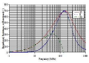
- Two-terminal AC loss versus frequency. This is given by the resistance plot “R” in Figure 1. It may be measured with or without applied DC bias. Nickel-zinc ferrites are intentionally used at frequencies where the resistive part of their impedance is dominant, whereas ferrites used primarily as cores in energy storage inductors and signal transformers are used at frequencies where the impedance is dominated by inductive reactance.
- “DCR” or DC resistance is measured under DC bias only, with no AC signal applied. This parameter allows the voltage drop at DC and AC power frequencies to be calculated for ferrites used as filter elements in power bus filters.
- “Volume resistivity”, determined by voltage drop per current density. This intrinsic property characterizes the current density induced into bulk ferrite material for a given applied voltage. This parameter is considered when ferrite is placed close to or in direct contact with two or more conductors that exhibit a potential difference, such as in electrical connectors or power transformers.
Only “1” and “2” are generally useful in the characterization and use of SMT ferrite devices. The maximum permissible current for a given device will be inversely proportional to its DCR. Current ratings for ferrites characterized by impedance are determined by the current that induces the maximum permissible temperature rise in the component.
Impedance vs. Frequency
Ferrite devices for PCB applications at frequencies above 30 MHz are most commonly manufactured with a ferrite material composed of iron oxide, nickel, and zinc. Most devices are characterized with an RF impedance analyzer to generate a swept frequency characteristic that displays magnitude of impedance versus test frequency. Figure 1 shows the impedance versus frequency characteristic of a 0805 package size two-terminal ferrite device intended for use in noise suppression applications above 30 MHz. As suggested by [4], [6], this characteristic can be modeled using lumped elements, whose peak impedance is pure resistance at the parallel resonant frequency. This characteristic demonstrates a frequency dependent loss and reactance, and can be divided into three regions; 1) Low frequency, high Q, since X=wL >> R, 2) mid frequency, low Q, and 3) high frequency, increasing Q as 1/wC > R. In Region 1 the magnitude of impedance is dominated by inductive reactance, in Region 2, by resistance, and in Region 3, the magnitude of capacitive reactance (not shown in Figure 1) eventually overtakes R.
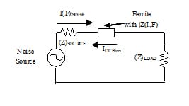
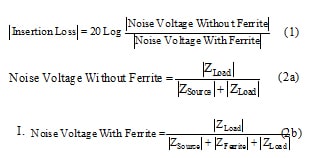
Since EMI is generally measured as a scalar quantity in decibels, a data plot showing only magnitude of impedance could at first glance be considered sufficient to generate an insertion loss prediction in conjunction with Figure 2 and:
 Most manufacturers of EMI suppression ferrites provide plots of impedance magnitude versus frequency for devices under zero bias. Since many applications require EMI suppression along conductors with net DC or low frequency power current, further characterization is necessary in order to predict and optimize noise reduction performance.

APPLICATION CIRCUITS WITH DC BIAS
Nickel-zinc SMT ferrites are commonly used as a series filter element in digital electronic design, placed between a DC power supply positive terminal and the power supply input pin of a high frequency digital integrated circuit, as shown in Figure 3. This application reduces the amplitude of the noise current and the resulting noise voltage induced by the integrated circuit along the power supply conductors. The impedance of the power bus is represented as ZPB. If the power supply conductors include attached wires with significant physical length compared to the noise frequency wavelength, then ZPB can also be considered to be the antenna input impedance for the power supply conductors when driven by noise currents. [8] From this discussion and Fig 3. a number of observations can be made:
- Noise suppression is maximum when the amplitude of the noise voltage at the power bus or antenna terminals is minimum. This condition occurs when the amplitude of noise current I(F)NOISE is minimum. Referring to (2b), for efficient antennas with low input impedance ZLOAD, noise voltage at the load is minimum at frequencies where the ferrite device impedance dominates both the noise source and antenna input impedance. The impact of the ferrite device can also be seen as a simple voltage divider between the noise source and its load.
- The ferrite device is placed under DC bias in this application. If its impedance versus frequency characteristic varies with DC bias, then noise attenuation in the circuit will vary with DC bias.
- For arbitrary digital electronic devices and arbitrary length power supply (bias) conductors, both noise current and antenna input impedance will be a function of frequency.

IMPEDANCE VS. DC BIAS FOR A SINGLE COMPONENT
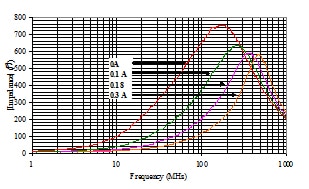
Figure 4 displays a family of curves that illustrate the impact of DC bias on the impedance versus frequency characteristic of a 0805 nickel-zinc SMT ferrite bead rated for use up to 500 mA. It is common practice in the EMC industry to use the approximate value of a ferrite’s magnitude of impedance at 100 MHz as a unique identification parameter; the part characterized by Figure 4 is therefore referred to as a “600 ohm ” device. The impact of increasing DC bias can be qualitatively summarized as follows:
- At frequencies below the zero bias parallel resonance, there is an apparent reduction in the two terminal series impedance presented by the device. At 100 MHz, a 200 mA DC bias through the device will result in more than a 50% reduction in impedance.
- The resonant frequency of the device increases.
- The quality factor Q increases as can be seen in
Figure 4. Higher bias levels create narrower peak responses. - At “very high” frequencies, peak performance at any bias level is generally within 3 dB of a zero bias peak.
The impact of increasing bias can be described as follows:
- EMI suppression will be inversely proportional to applied DC bias at frequencies below the zero bias parallel resonance.
- Low frequency EMI suppression is greatly reduced at higher bias levels. At higher frequencies, Q increases and the device’s different impedance versus frequency versus bias characteristics converge.
- For electronic systems where DC and AC power supply currents are determined by the type and number of scaleable hardware options installed, the number of noise sources and power supply current will increase simultaneously. An increase in total system noise amplitude may be associated with the addition of active circuitry when the root cause is actually a reduction in filter performance due to increased DC bias.
EFFECTS OF BIAS A S FUNCTION OF SMT PACKAGE SIZE AND DEVICE SELECTION FOR A GIVEN APPLICATION
When ferrite devices are selected for DC power bus EMI filter applications, the most common device performance criteria are 1) adequate DC current rating and DCR, 2) maximum impedance, 3) minimum package size consistent with PCB assembly technology, and 4) cost. The manner and priority with which criteria 1, 2 and 3 are considered can have a profound effect on the choice of device and resulting noise filter performance.
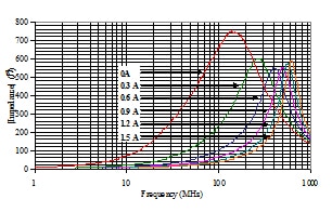
Suppose a design application requires a high frequency ferrite for filtering 300 mA of digital logic supply current. How then should a designer select a part for maximum noise attenuation if there are three “600 ohm” devices available with the following package sizes & current ratings; “#1” = 0603, 300 mA, “#2″= 0805 (500 mA), and “#3″= 0805 (1.5A). We assume that all three devices have sufficiently similar zero bias impedance versus frequency characteristics and acceptable DCRs for the given application. Figures 4, 5 and 6 give impedance versus frequency versus bias data for these three devices.
The effect of 300 mA of bias is tabulated at the frequency of peak impedance under zero bias Fo and presented in Table I. Also summarized is the effect of maximum rated bias current and its associated frequency of peak impedance Fm. Note that these maximum currents are significantly different for each device, yet the peak impedances demonstrated by each device under maximum bias are remarkably similar. If the maximum bias peak impedances were normalized to account for the approximately 50 ohm greater zero bias peak impedance of devices 1 and 3, the maximum value peak impedances would differ by less than 2%! Since Fo and Fm, do not vary much among the three devices, we can consider a “low” frequency ranges up to and including the highest zero bias Fo, and a high frequency range beyond the highest Fm. At low frequencies the largest device with highest current rating provides maximum impedance. But when placed under 300 mA of bias, its impedance at its zero bias resonance frequency declines by 55% when compared to its zero bias value. At maximum bias, all three devices exhibit a maximum impedance within 25% of their peak impedance at zero bias, an insignificant change in the context of noise suppression measurements units of decibels. At frequencies near and above Fm for any device there is much less change in peak impedance with frequency.
CONCLUSIONS
- Larger package size in general maintains a greater percentage of zero bias impedance at frequencies below zero bias resonance.
- To yield maximum noise suppression in real applications, devices must be characterized for impedance versus frequency over the range of expected bias levels.
- The frequency of maximum impedance can be “tuned” by the application of a fixed DC bias.
- Many application circuits apply a bias current. Manufacturer’s impedance characterizations at zero bias are insufficient for predicting performance, even in applications with bias levels below 300 mA.
- At “high” frequencies, a device’s peak impedance is much less sensitive to bias and will maintain a greater percentage of its claimed zero bias impedance.
- A device’s high current rating and/or large package size does not necessarily alleviate DC bias effects on its impedance.
ACKNOWLEDGEMENTS
The authors thank Arlin Grant and Aaron Fitzsimmons of Steward for supporting this project and providing plenty of data, and Randal Vaughn of SILENT for manuscript review.
REFERENCES
[1] C. R. Paul, Introduction to Electromagnetic Compatibility. New York: John Wiley & Sons, 1992.
[2] H. W. Ott, Noise Reduction Techniques In Electronic Systems, 2nd ed. New York: John Wiley & Sons, 1988.
[3] D. L. Terrell and R. Keenan, Digital Design for Interference Specifications, 2nd ed. Pinella Park, Florida: The Keenan Corporation, 1997.
[4] W. D. Kimmel, “Wide Frequency Impedance Modeling of EMI Ferrites”, in Proc. IEEE EMC Symposium,
[5] Digital Design for Interference Specifications, 2nd ed. Pinella Park, Florida: The Keenan Corporation, 1997.
[6] Q. W. Yu, W. Holmes, and Krishna Naishadham, “RF Equivalent Circuit Modeling of Ferrite-Core Inductors and Characterizations of Core Materials”, IEEE Trans. Electromag. Comp.”, vol. 44, no. 2, pp 258-262, Feb 2002.
[7] K. Naishadham, “A Rigorous Experimental Characterization of Ferrite Inductors for RF Noise Suppression”, in Proc. IEEE RAWCON., Denver, CO, Aug. 1999, pp. 271-274.
[8] M. Li, X. Luo, and J. Drewniak, “FDTD Modeling of Lumped Ferrites”, IEEE Trans. Electromag. Comp.”, vol. 42, no. 1, pp 142-151, May 2000.
[9] T. Hubing and J. F. Kaufman, “Modeling the Electromagnetic Radiation From Electrically Small Table-top Products,” IEEE Trans. Electromag. Comp.“, vol. 31, pp. 74-84, Feb. 1989.
