NOTE: This article has been translated from French into English. It can be found in its original language in the 2014 EMC Europe Guide.
Sébastien Serpaud, EMC Design Support, NEXIO, Toulouse, France; sebastien.serpaud@nexio.fr
Sebastien Ocquidant, EMC Specialist, EATON, Montbonnot St. Martin, France; sebastienocquidant@Eaton.com
Jean-Philippe Tigneres, EMC Specialist, BARCO, Toulouse, France; jeanphilippe.tigneres@barco.com
CONTEXT
In electronic design phases, EMC is largely responsible for cost overruns and schedule changes. Often, EMC experts do not have all the necessary tools to improve design before the final stages of validation. Feedback from previous experiences is often the best input in these situations. In order to try and address this problem, six years ago we started working on the development and improvement of a testbed based on the technique of near field measurement.
INTRODUCTION
The common method to measure radiated emissions employs an antenna to capture the “far-field” emitted by the device under test. All standard qualification tests are based on this method. The electromagnetic (EM) field in the far region could be summarized by a planar waveform propagating in the free space, with wave impedance of 377 ohms. In this case, all information about the source is lost and only the magnitude of the field is saved. This approach gives relevant information to help qualify for EMC compliance, but does not help to identify the origin of the disturbance.

The near-field measurement technique is affected very little by external disturbance. The near-field measurement set-up is simpler than that of the far-field measurement due to the fact an anechoic chamber is not necessary. In addition, the measurement cost and time is reduced and the reproducibility of measurement is better, shortening the investigation time.
In the following section, the common near-field measurement technique applied to an industrial case study is discussed.
NEAR FIELD MEASUREMENT TECHNIQUE – CASE STUDIES
A lot of papers present this measurement technique [1][2][3]. As a reminder, the set-up to measure the magnitude of field is performed by a spectrum analyzer (SA) connected to the near field probe as described in Figure 1. A low noise amplifier (LNA) can be used to increase the signal to noise ratio (SNR).
In the following part of this paper, we will illustrate the added value of the near-field measurement technique on some industrial case studies.
Case 1: Investigation of Radiated Emission Problems on an Electronic Board
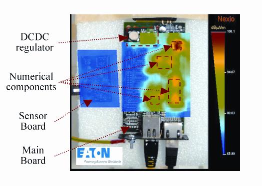
The study presented below shows an investigation done by Nexio on product of Eaton Society. Initially, a study based on the GTEM method was performed and a design issue was found on the sensor board (the small board on the left of the picture in Figure 2).
Then, a near field investigation was performed. The result of this study is presented in Figure 2. A short summary of this study is given below:
- No radiated emission was measured on the small board.
- Several emission peaks were observed over digital components.
- Digital activity was visible above the DCDC regulator.
- A poor ground connection of the DCDC regulator was identified
- The main and sensor boards are linked with shielded cable
- The ground plane was not connected with the shielding.
Summary point 1 (above) concludes that the sensor board is not the disturbance source. Points 2, 3 and 4 show that the decoupling network of digital components is not optimal and generates broadband activity on the power distribution network (ground bounds). Points 5 and 6 present a good propagation path (antenna effect) of the digital interference visible on the standard EMC test.
With this example, we show that the general analysis done by the standard EMC test cannot always precisely identify the design issues on an electronic board. Without a specific investigation tool, it is very difficult to localize the real EM perturbation source. Often that is the consequence of disturbance (here antenna effect) that is localized.
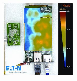
Figure 3 shows a second measurement done nine months after the first. Between the two measurements, some corrections were implemented. This second analysis showed a reduction of emission levels from digital sources (-1.5 dB) and the DC / DC converter (-5 dB).
In conclusion, this study shows that an investigation (2×1 days) based on the near field measurement can quickly and precisely identify emission sources responsible for non-compliance EMC. Note here the very good reproducibility of the measurement in the near field. Comparing the two measures, we find a difference of only 0.3 dB over the unmodified design parts.
Case 2: Default Production Casing of a Hardened Military Computer
The study presented below shows an investigation done by Barco on one of its military rugged computers. Military standards for radiated emissions are very harsh in comparison to EN standards. Barco designed this computer in order to minimize radiated emission levels, particularly in the 30-88 MHz radio band. EMI sources present in the 30-88 MHz band can drastically affect the digital radio military network propagation distance range if near the emission antenna. To avoid this, the electronic devices installed in the vehicle / boat / plane near the antenna must be designed with a very low level of radiated emissions. The design and qualifications were done by Barco and were compliant to these specifications.
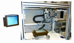
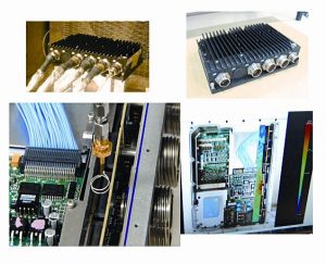
Then the manufacturing was moved to Asia and non-regression testing was used. One of the most important test phases in such a case is radiated emission measurement in an anechoic chamber. Barco found some big problems between 30 and 1000 MHz, including in the military radio band. A near-field investigation was performed using Nexio 3D scanning capabilities.
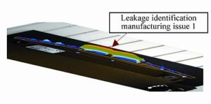
The near field measurement allowed the engineers to quickly and accurately identify manufacturing defects of the computer case by highlighting radiated emission leaks, as the results show in Figure 5. In just one day of testing, this study was much less expensive than a study in an anechoic chamber.
After locating the area of low shielding effectiveness of the case, a second analysis was performed that same day. The equipment was opened and a near field measurement was performed on each part of electronics boards.

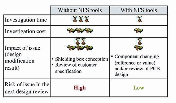
Identifying both the areas of low shielding effectiveness and the disturbance sources make it easier to reduce emission levels. Locating the area of low shielding effectiveness can help specify a new case or correct the original one, but this can be time consuming and costly. The identification of the disturbance sources allows work at board level, enabling the correction(i.e. maximizing the value of decoupling capacitor, filters, embedded software, or as a last resort a local internal shield) to be faster and cheaper.
Case 3: Radiated EMC Design Issues on a Military Rugged Computer
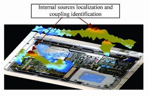
The following continues the investigation done by Barco on one of its military rugged computers. During the design phase, one EMC issue was found for a specific test setup condition and it was difficult to identify root cause. The design and the qualification were done by Barco and were compliant to the specification, except the issue with the specific test setup condition. To identify the weaknesses in the EMC design, near-field investigations were performed using Nexio 3D scan capabilities.
The near-field measurement allowed engineers to quickly and effectively identify the design problem (internal coupling transmitted by external cables.) The identification of internal EMI sources allowed for the development of solutions to reduce coupling (shielding, filtering and software.) This one-day study was much less expensive than a study in an anechoic chamber, which may not have even led to the identification of actual sources. The solution would have probably been use of a shielded cable, a solution that would mean additional cost and time requirements.
CONCLUSION
In this paper we have described three industrial case studies that employed the near-field scanning method to investigate issues at the equipment and system levels. These studies show that the near field scanning method is very important to solving localized issues of electronic board design. While not foolproof, this method can provide a powerful tool for investigating EMC issues in the design of electronic circuits.
To reiterate, the benefits of near-field measurement are:
- Low cost (anechoic chamber is not required)
- Not dependent setup (only the product is measured)
- Non-invasive method (Non-contact)
- High reproduction ability ( Identification of the real root causes of disruption
- Wideband: 10kHz-5 GHz (can be extended further)
Another benefit of using near-field measurement is that the real issue is more easily found with this investigation tool. Valuable time is saved and the design is secured for re-use in future projects.
ACKNOWLEDGEMENT
I would like to thank the Eaton and BARCO companies for agreeing to share the results of investigative studies performed on their products.
REFERENCES
[1] Jin Shi, Michael A.Cracraft, Jianmin Zhang, Richard DoBroff,”Using near-field scanning to predict radiated fields”, IEEE, EMC 2004 International Symposium, 14 – 18 vol.1, 9-13 Aug. 2004
[2] Adam Tankielun, Uwe Keller, Etienne Sicard, Peter Kralicek, Bertrand Vrignon, “Electromagnetic Near-Field Scanning for Microelectronic Test Chip Investigation”, IEEE EMC Society Newsletter, Collection IEEE EMC, Octobre 2006
[3] D. Baudry, A. Louis, B. Mazari, “Overview of emission and susceptibility investigation and modeling with near-field measurements.”, URSI GA 2008, Chicago, USA, August 2008
[4] S.Serpaud, L.Arnal, B.Ravelo, D.Baudry, “Conception Assistée par Mesure en Champ Proche“, Workshop 2EMC 2010, Rouen
[5] “Technical Improvement of the Near Field Measurement: The Vector Near Field Scanning”, Sébastien Serpaud, Samuel Leman; EMCEurope2013, Septembre 2013, Brugge, Belgium
