Co-authored by: Kenneth Wyatt and Steve Sandler
INTRODUCTION
Modern devices are continuing a long-term trend of squeezing more electronics into smaller packages, while also increasing system performance, data rates and operating efficiency. Higher efficiencies are often achieved by implementing faster silicon MOSFETs or even faster eGaN FETs while size is reduced by increasing switching frequencies and replacing aluminum and tantalum capacitors with smaller ceramic devices. One result of this trend is that there is greater interaction between the disciplines of EMI, signal integrity (SI) and power integrity (PI).
EMI is a measure of the electromagnetic emissions produced by the high-speed current and voltage signals the system creates. Power integrity is a measure of the power quality at the device that being powered. This means that the power supply voltages must be maintained within the allowable operating voltage range of high-speed devices. Devices, such as modems, reference clocks and low noise amplifiers (LNAs) are all sensitive to noise on the power rails, which results in timing jitter, spurious responses reduced data channel eye openings, and degraded signal-to-noise ratio (SNR). This too, is a measure of power integrity. The power supply itself is a noise source and the noise sources generated by the power supply must be kept from propagating through the system.
This article discusses the three most common causes of EMI and power integrity issues while providing tips for how to avoid or minimizes them in your design,
- Ringing on switched waveforms causes broad resonant peaks in the emission spectrum.
- DC-DC converters generate noise at the switching frequency, and because of high speed switching devices, can generate broadband switching harmonics well into the GHz.
- Power plane resonance in DC-DC converter or LDO regulators due to high-Q capacitors resonating with power planes.
RINGING AND RADIATED EMISSIONS
Any ringing on the switched waveform (fairly common) can lead to broadband resonances in the resulting RF spectrum. Resonant frequencies resulting from DC-DC converters or low dropout (LDO) linear regulators can be as low as a few kHz while resonance due to the PDN with switching devices, such as MOS-FET’s can be in hundreds of MHz or higher.
The harmonic energy resulting from this switching is “captured” by the PDN and device resonances, evident as ringing in the time domain. The current and voltage of this ringing produces EMI. The magnitudes of the ringing and EMI are related to the quality factor (Q) and characteristic impedance of the resonance and the harmonic energy produced by the switching.
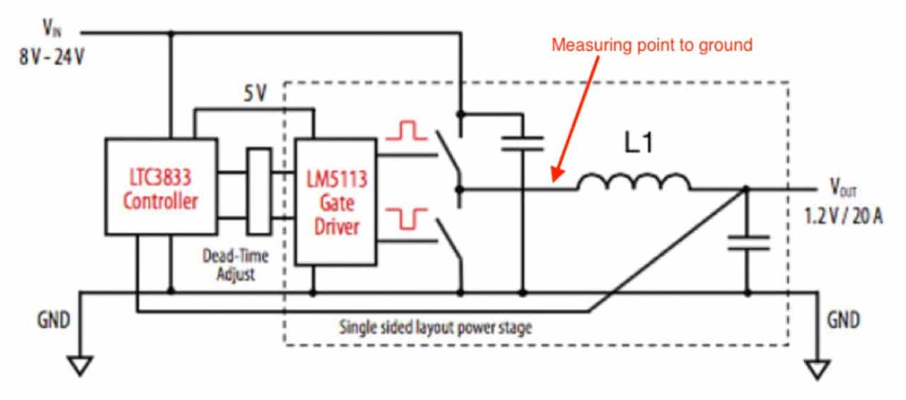
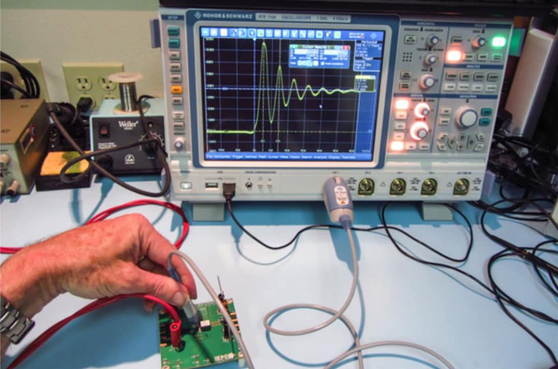
As an example, the switching waveform on a DC-DC buck converter demo board was measured with a Rohde & Schwarz RTE 1104 oscilloscope and Rohde & Schwarz RT-ZS20 1.5 GHz active probe (Figure 1).
There was a very large ringing superimposed on the switched waveform of 216 MHz. This can be seen clearly in Figure 2.
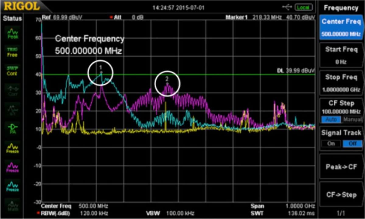
A Fischer Custom Communications F-33-1 current probe was used to measure both the input power cable common mode cur-rent (violet trace) and output load differential mode current (aqua trace). See Figure 3. Note the broad resonant peaks at 216 MHz (marker 1) and the second harmonic at 438 MHz (marker 2).
Remediation Tips – There are several ways to improve the design to minimize the resonances, ringing and therefore EMI. Since the energy is related to the switching frequency, rise time of the switching, characteristic impedance, and Q of the resonances, these factors are also the paths to mitigation.
- Slower edges will degrade operating efficiency but reduce high frequency energy
- Careful PCB design and capacitor selection will minimize the characteristic impedance and Q
- Keep traces short and wide and dielectrics thin.
- Keep all the switching circuitry on one side of the board, prefer-ably with a thin dielectric to the respective ground return plane.
- Use of a snubber circuit, damping of resonances using con-trolled ESR capacitors, or redesign of the inductor for lower leakage inductance.
For additional detail on measuring ringing refer to Reference 1.
FAST EDGES CREATE BROADBAND NOISE AT GHZ FREQUENCIES
Today’s on-board DC-DC converters use switching frequencies as high as 3 MHz. This is an advantage because it allows for physically smaller inductor and filter components, as well as increased efficiency. However, the fast edge speeds create broadband harmonic energy. The bandwidth of this harmonic energy is related to the voltage and current rise time. A 1ns edge speed can produce harmonic energy up to 3 GHz, or more.
These broadband harmonics are the cause of radiated emissions failures and also can affect the receiver sensitivity of any on-board telephone modems or other wireless systems, such as GPS. Figure 4 shows how a typical DC-DC converter circuit can be characterized using an H-field probe connected to a spectrum analyzer.
It’s also possible to connect the probe to an oscilloscope and hold it near each DC-DC converter to get some idea of the ringing, if any, without disturbing the circuit.
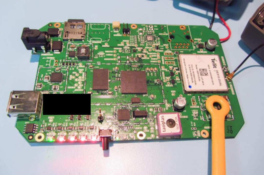
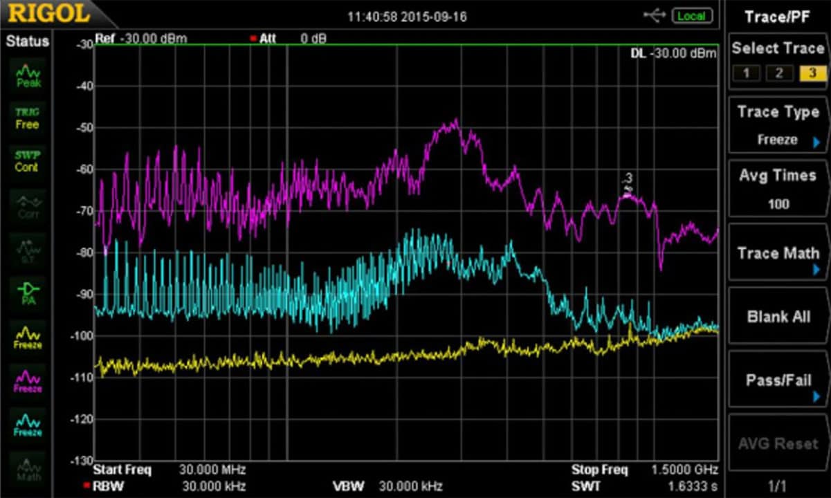
Figure 5 shows the resulting measurement of a couple DC-DC converters. The yellow trace is the ambient noise floor of the measurement system and is always a good idea to record for reference. The aqua and violet traces are the two converter measurements. Note that both produce broadband noise currents out to 1 GHz, with the convertor in violet out to beyond 1.5 GHz. Note the violet trace is 20 to 50 dB higher than the ambient noise floor.
Remediation Tips – To reduce the risk of self-interference to on-board mobile phone modems and wireless systems, the product design must start off with EMC in mind and with no corners cut.
This will consist of:
- A near perfect PC board layout
- Filtering of DC-DC converters
- Filtering of any high frequency device
- Filtering of the radio module
- Local shielding around high noise areas
- Possibly shielding the entire product
- Proper antenna placement
The PC board layout is critical and is where most of your effort should reside. An eight or ten layer stack-up will provide the most flexibility in segregating the power supply, analog, digital, and radio sections and provide multiple ground return planes, which may be stitched together around the board edge to form a Faraday cage. Care must be taken to avoid return current contamination between sections – especially in the ground return planes. For wireless products, the power plane for the radio modem section should be isolated (except via a narrow bridge) from the digital power plane. All traces to this isolated plane should pass over the bridge connecting the two. This can provide up to 40 dB of isolation between the digital circuitry and radio.
It is vital that the power and ground return planes be on adjacent layers and ideally 3-4 mils apart at the most. This will provide the best high frequency bypassing. All signal layers should be adjacent to at least one solid ground return plane. Clock, or other high-speed traces, should avoid passing through vias and should not change reference planes.
Power supply sections should be well isolated from sensitive analog or radio circuitry (including antennas). Be aware of primary and secondary current loops and their return currents. These return currents should not share the same return plane paths as digital, analog, or radio circuits. Remember that high frequency return currents want to return to the source directly under the source trace.
For more details on resolving DC-DC converter noise issues with wireless radio modems, refer to Reference 2.
PC BOARD PLANE RESONANCE AND THE EFFECT ON RADIATED EMISSIONS
Noise propagation in a simple system can be represented by three elements, the voltage regulator, the printed circuit board planes with decoupling capacitors (PDN) and the device being powered (load).
Each of these three elements is comprised of resistive, inductive and capacitive terms. Even “noise free” low dropout (LDO) regulators can be highly inductive (Reference 3). The resistive, inductive and capacitive terms can resonate amplifying the noise signals created by the power supply and the load as they travel across the PDN creating EMI. The harmonics of the switching frequency and the switch ringing discussed earlier excite these PDN resonances (Reference 4). As stated previously this noise can degrade and interfere with on-board wireless modems, as well as resulting radiated and conducted emissions.
A short video helps explain the basic principles of PDN design (Reference 5). The radiated EMI of a LTC3880 DC-DC converter measured near the input plane using an H-field probe is seen in Figure 6.
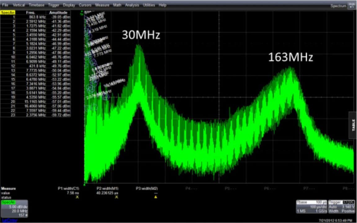
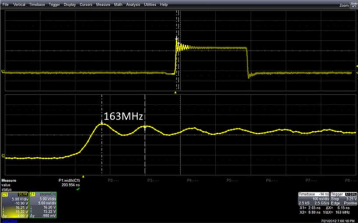
The 163 MHz is attributed to the ringing of the switches as seen in Figure 7. This ringing is caused by the inductance of the upper MOSFET bond wires, pins and circuit board planes, ringing with the lower MOSFET and PC board capacitance.
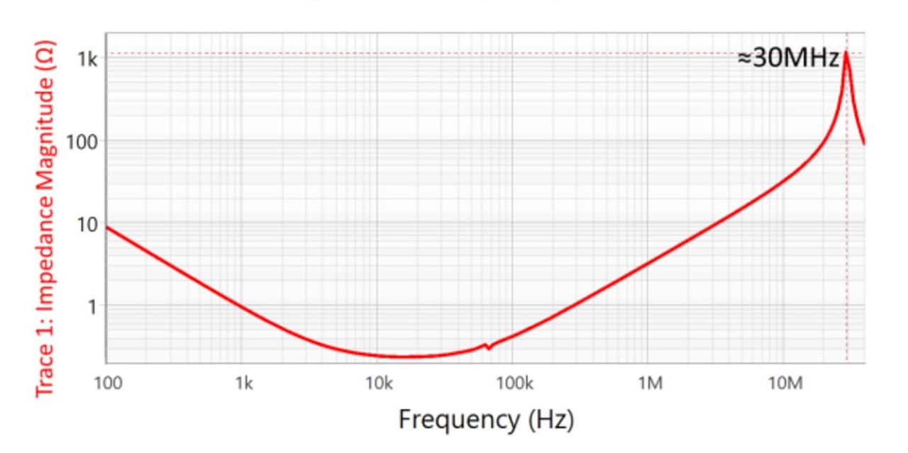
The input ceramic decoupling capacitor resonates at approximately 30 MHz, as seen in Figure 8 and results in the large 30 MHz EMI signature.
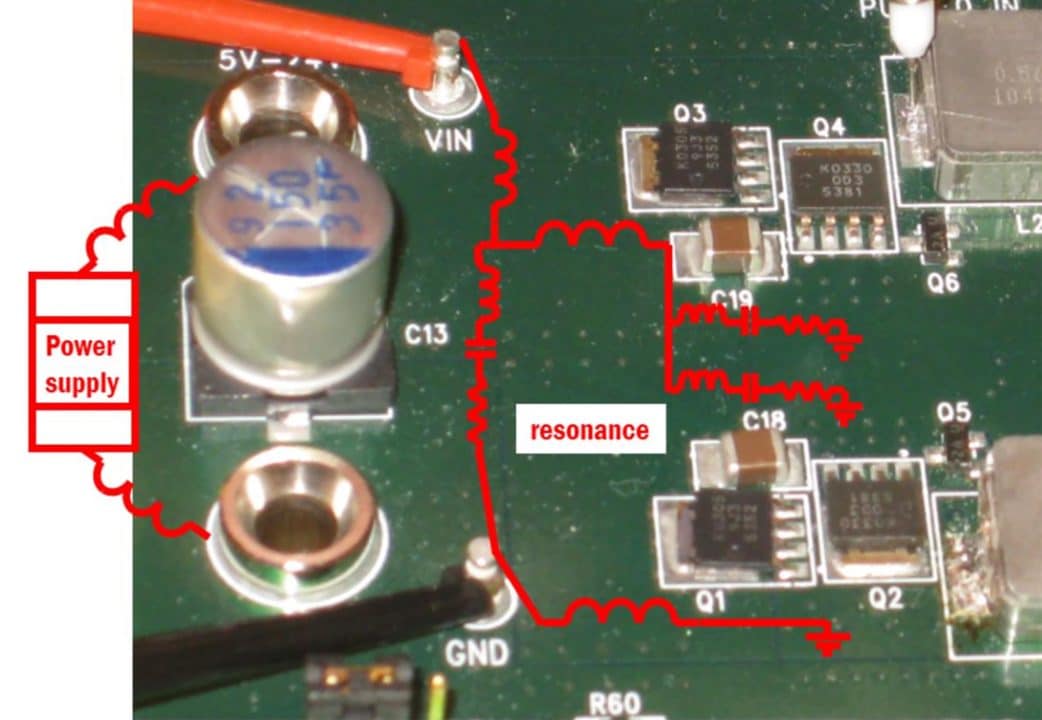
The input power plane section of the DC-DC converter (measured in Figure 6) is shown in Figure 9 with schematic representations of the component, PC board and external connections.
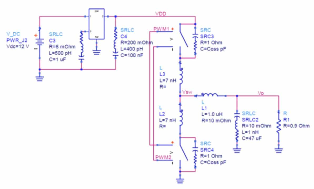
A very simple simulation example can be used to illustrate these impedance resonance effects. Consider a simple DC-DC converter as shown in Figure 10.
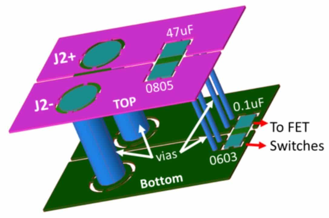
Designers frequently place the FET switches on one side of the board with power entry on the opposite side of the PC board. The small PC board plane used in this example has power entry through a pair of pins and no interconnect inductance is added to connect power to the PC board. A large 47 μF ceramic capacitor is placed on the top side of the PC board, while a smaller, 0.1 μF ceramic capacitor is placed very close to the FET switches on the bottom side of the PC board. Two parallel vias connect power and ground from the top side of the PC board to the bottom side as seen in Figure 11.
The simple model is used to simulate the harmonic current in the input connector, which is directly related to conducted and radiated emissions. Two simulations are performed; one with low ESR ceramic capacitors and the other with a lower Q controlled ESR ceramic replacing the 0.1 μF capacitor close to the FET switches. Both simulations are shown together in Figure 12.
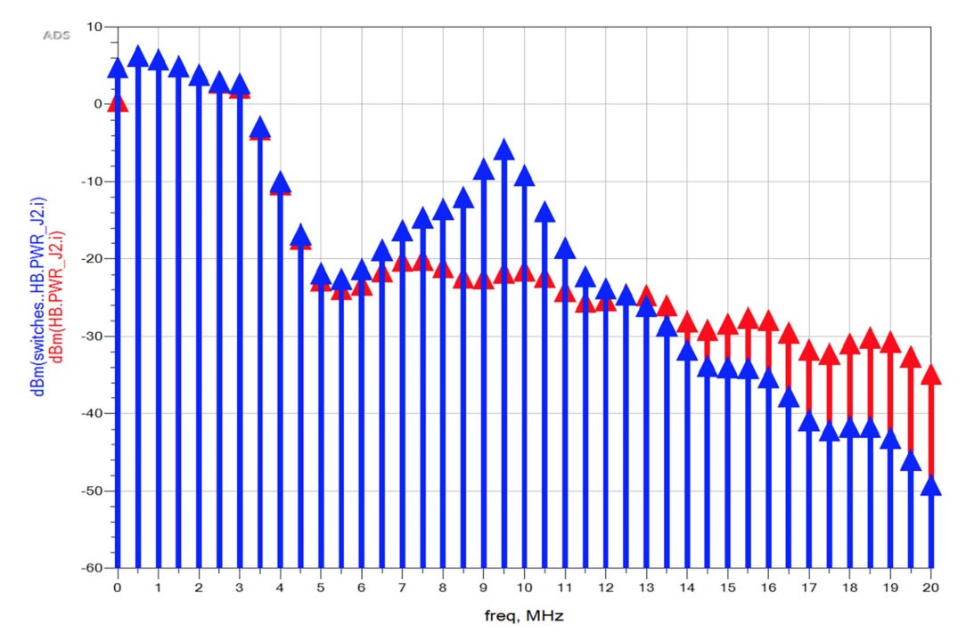
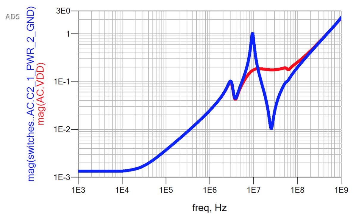
The simulated impedance, measured at the smaller capacitor in Figure 13 shows the corresponding plane resonance with a clear 10 MHz peak using the high Q ceramic capacitor (blue) and the peak is eliminated using the controller ESR ceramic capacitor (red).
Remediation Tips – To minimize PDN resonances, the complete system of voltage regulator, PDN and the load need to be carefully balanced. Damping resistance must be included to eliminate or minimize the existence or Q of resonances. This will consist of:
- Short, wide power planes
- Keep the layout as small as possible to minimize inductance
- Thinner PC board dielectric layers, closer to the surface
- Incorporate EM simulation to identify and minimize PDN resonances
- Keep capacitors on one side of the PC board to the extent possible
- Low-Q or ESR controlled capacitors reduce Q
- Choose voltage regulators and output capacitors for good control loop stability
- Don’t place cutouts or holes in ground plane layers below the power plane
- Ferrite beads are a very common cause of PDN resonances
- Be aware of inductive interconnects bringing power to the system.
Printed circuit board design and decoupling is critical and “rules-of-thumb” generally don’t work well in high speed circuits. The design of the circuit board and capacitor decoupling always involves trade-offs, but the impacts on resonances need to be weighed carefully. A multi-frequency harmonic comb generator can be extremely helpful for quickly identifying PDN resonances (Reference 3).
SUMMARY
As you can see, designing DC-DC converters, LDOs, and PDNs with today’s high-speed technology nearly always requires careful circuit design, adequate filtering, simulation of the PDN, very careful circuit board layout, and use of controlled-ESR filter capacitors. Poor designs can result in:
- Ringing in power supply switches (or other fast-edged digital switching) resulting in associated radiated or conducted emissions resonant peaks at the ring frequency and harmonics.
- High frequency broadband noise well beyond 1 GHz, resulting in self-interference to radio modems.
- Poor stability and resonances in undamped power distribution networks, leading to instability, spectral resonances, and associated radiated and conducted emissions.
REFERENCES
- Wyatt, GaN Technology and the Potential for EMI (EDN), http://www.edn.com/electronics-blogs/the-emc-blog/4439839/GaN-technology-and-the-potential-for-EMI
- Wyatt, Platform Interference (EDN), http://www.edn.com/electronics-blogs/the-emc-blog/4441086/Platform-interference
- Wyatt, Review: Picotest J2150A Harmonic Comb Generator http://www.edn.com/electronics-blogs/the-emc-blog/4440532/Review–Picotest-J2150A-harmonic-comb-generator
- Sandler, The Inductive Nature of Voltage Control Loops, http://www.edn.com/electronics-blogs/impedance-measurement-rescues/4438578/The-inductive-nature-of-voltage-control-loops
- Sandler, How to Design for Power Integrity: Finding Power Delivery Noise Problems (Video), https://www.youtube.com/watch?v=oL6qjhJH_m4&t=4s&list=PLtq84kH8xZ9HIYg-BYDsP7TbqBpftidzI8&index=4
Steve Sandler, CEO of Picotest Systems, has been involved in high reliability electronics for nearly 40 years. He is the author of numerous articles relating to power integrity and distributed systems. He is also the author of SMPS Simulation with SPICE 3, Switch-Mode Power Supply Simulation: Designing with SPICE 3, and the co-author of SPICE Circuit Handbook, all available from McGraw-Hill. His most recent book, Power Integrity – Measuring, Optimizing, and Troubleshooting Power Related Parameters in Electronic Systems, was released in 2014 from McGraw-Hill. Mr. Sandler lives in Phoenix, Arizona, and may be contacted at steve@picotest.com.


