Evaluation of a dual-line filter by measuring and modeling over a broad range of frequencies involves a number of complexities.
James P. Muccioli and Dale Sanders, Jastech EMC Consulting, Farmington Hills, Michigan, USA
INTRODUCTION
When evaluating the performance of an EMI filter, there are several ways to approach the test methodology. For single-ended components such as capacitors and inductors (lumped elements), a two-port network analyzer can perform a very accurate broad frequency characterization of components. These characterizations can prove valuable when building accurate circuit models. Still, when evaluating a dual-line filter, the complexity of measuring and modeling a filter’s performance over a broad frequency can produce results that differ substantially from real world out comes.
For accurate determination of common mode and differential mode noise performance on a dual-line filter, the circuit designer needs to understand the parasitics associated with the circuit, as well as the parasitics associated with the EMI filter. Parasitic variances induce impedance imbalance between lines as well as to the circuit’s reference (ground). To compensate for parasitic imbalances, it generally requires a complex EMI filter design resulting in larger values of lumped elements (capacitance and inductance). A properly designed and implemented EMI filter will balance a circuit’s parasitic impedance mismatch to combat common mode and differential mode noise, as well as the conversion from one to the other. The scope of this article is to propose a test methodology that will determine the balance and parasitics of an EMI filter both in and out of a circuit.
WHAT IS BEING MEASURED?
The first step in evaluating an EMI filter is to determine what is being measured and what information is important. To simplify these questions, an engineer can classify measurements in one of three ways.
-
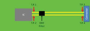
Figure 1. “System classification” measurement. Notice that the test points are located at the IC and the connector. 
Figure 2. “Filter-in-system classification” measurement. Notice that the test points are located just before and after the EMI filter. System classification – shows the net result of adding an EMI filter to a circuit’s loop that measures the total impedance of the filter plus physical geometries such as PCB layout, vias, and plane spacing. For example, Figure 1 has an IC driving a differential signal pair to a connector at the edge of a PCB. Test points pairs should be located at the pins of the IC and at the pins of the connector. The net impedance includes the total impedance from both the filter and the PCB.
-
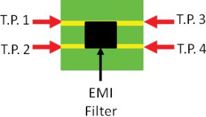
Figure 3. “Filter-only classification” measurement. Notice that the test coupon is just big enough for the EMI filter and connectors. Filter-in-system classification – this measurement would be the same as “system classification” except that it measures only the impedance of the filter and the filter’s loop on the PCB. Figure 2 shows that test point pairs would be located just before and after the filter. The net impedance includes parasitics from the filter and its mounted loop.
- Filter-only classification – a specifically designed test coupon is used to measure an EMI filter outside of the intended circuit where all fixture and circuit parasitics can be removed. The net impedance includes only the filter’s parasitics (Figure 3).
It is important to note that classifications can overlap; however, this overlapping does not present a significant problem as long as parameters such as those listed below are fully defined and agreed upon.
- Test fixture setup/layout
- Location of test points
- Number of components that comprise the filter
TEST COUPON DESIGN FOR FILTER-ONLY MEASUREMENTS
A test coupon has many factors that can significantly affect measurements and these will, of necessity, affect correlation to other measurements. Most component/filter manufacturers supply information such as insertion loss curves or impedance measurements for their products. Unfortunately, no standard exists to control how this data is obtained. Evaluation of products from various manufacturers, or even different product lines from the same manufacturer, can pose an impossible challenge if further information is not available. The designer must determine how the test fixture was constructed, obtain a description of the test setup, find the type of calibration employed, and learn the size of the sample base. If additional information about manufacturer’s data is not available, then the engineers must determine if they will accept the data, or will need to perform a validation test of their own.
The good news is that test coupons, with a little thought, can be constructed very inexpensively and can provide good performance insight for most filter evaluations. Considerations for any good test coupon should be the frequency range of interest and the type of measurement classification desired. Defining these things will help determine test coupon’s parameters including dielectric material; its shape and size (length, width, and height); and its layout, construction, and test points.
NETWORK ANALYZER CALIBRATION, SETUP AND FIXTURE EXTENSION
Prior to performing a calibration on the network analyzer, the setup, channel, and state should be loaded. The setup should include start and stop frequency, measurement bandwidth, number of points, channel and trace setup, and type of measurement (e.g., balanced pair measurement). “Balance pair measurement” is also known as mix-mode or infinite balun measurement. (In the following discussion, the term “mix mode measurement” will be used.)The mixed mode measurement determines the common mode (CM) and differential mode (DM) responses, as well as the conversion responses—i.e., common-to-differential (CD) and differential-to-common (DC). (Mix-mode measurements are similar to using physical baluns without the calibration difficulty or frequency limitations.[1])
Another item to be aware of when using four-port network analyzers is the manner in which mix mode measurements are taken. In a “virtual” mix-mode, a signal is sent out one-port at a time. The CM, DM, DC, and CD responses are then calculated using software. In a “true” mix-mode, a true differential signal is sent out on two-ports simultaneously. Actual hardware is used to measure CM, DM, DC, and CD. (The cases for “virtual” and “true” mix-mode are explored in the example below.)
The calibration of a network analyzer usually includes the test cables as a minimum. This process can be carried out with either a manual calibration kit (through-open-short or through-open-short-matched) or with an electronic calibration device. Either method will result in a highly repeatable calibration of the network analyzers and cables. Still, depending on the classification of measurement being taken (system, system-in-filter, or filter-only), some thought should be given to include calibration of the test coupon and/or any probes attached to the test cables.
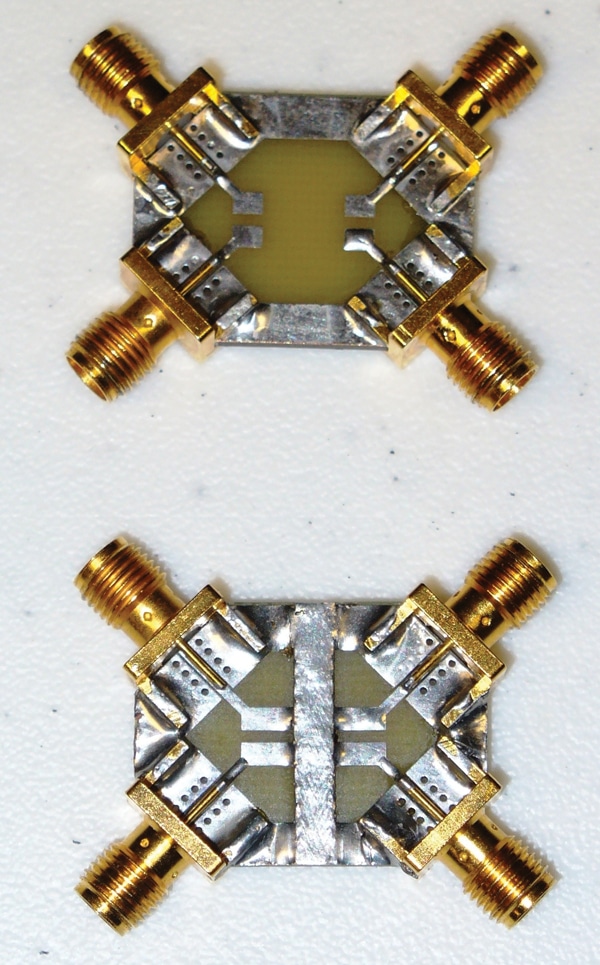
Extending the calibration plane to the test fixture (coupon) can be done by simply applying an “open” and “short” correction. The procedure for applying this correction can be found in the application notes supplied by manufacturers of network analyzers.[2] Examples of “open” and “short” coupons are shown in Figure 4.
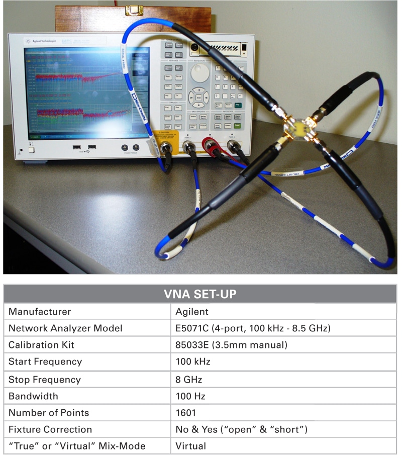
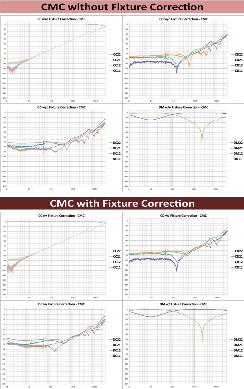
To demonstrate the difference between a mix-mode measurement with and without a test fixture (coupon) correction, see Figure 5 and Figure 6. Figure 5 shows the test layout and equipment setup, and Figure 6 shows the results of a common-mode-choke with and without a test fixture correction. As shown in the data, applying the coupon correction has a very noticeable effect on the two conversion measurements CD and DC.
AUTOMOTIVE CANBUS CMC EVALUATION EXAMPLE
This example was chosen to highlight the key testing concepts under discussion and to show how to apply the test methodology in a practical application that has a unique set of parameters. Before any discussion of data, several vital steps are crucial. These include identifying application criteria, determining the parameters, setting the goals, and defining the test setup.

Application criteria
For example, consider the application criteria and the unique challenges when applying EMI filters in an automotive CANBus application. As more and more integrated electronics have been added in automotive applications, the number of CAN nodes on vehicles has increased as well. Increased nodes mean faster transmission speeds and more capacitive loading of the bus. CAN protocol speeds have increased from 250 kbps to 500 kbps to 1 Mbps, a change that also increases signal rise and fall times. Faster rise and fall times increase the frequency content that may require filtering.
Total capacitance on the CANbus is a collective value of all the nodes. Too much capacitance can affect signal integrity. Automotive OEMs specify a maximum capacitance value for each node. Typically, it is between 56 and 100 pF. This range directly affects EMI filter design. Line-to-ground capacitance for each line is also important since CAN is a differential signal. Any imbalance between the line-to-ground values can degrade signal transmission. Some automotive OEMs mandate the use of a common-mode choke (CMC) for EMI filtering although other discrete components are usually needed to handle higher frequency content, transients, or immunity criteria. Component manufacturers that supply CMCs for automotive applications specify only an impedance value at a particular frequency. Parasitic capacitance is not specified nor is line-to-line impedance balanced.
Finally, it should also be noted that most automotive electronic applications use either a two-or four-layer FR-4 PCB (62-mil thick) to minimize costs. This limits the amount of impedance control that can be achieve on the PCB as well as options to maximize EMI filter design and implementation.
Determining the parameters
As noted above, component manufacturers for the CANBus CMC do not give specifications for parasitic capacitance or for line-to-line impedance balance. This example, therefore, will look to measure these parameters. The type of measurement classification will be “filter-only” because the PCB parasitics and the total incorporated circuit loop will mask the true information being sought.
Since most automotive EMC requirement levels are between 150 kHz and 3 GHz for emissions, this will be the frequency range of interest. With this requirement defined, using an FR-4 (62-mil thick) two-layer PCB with end-launch SMAs, a test coupon can be constructed. Figure 7 shows the constructed coupons, as well as the layout. Notice the SMA end launch is designed for 50-Ω impedance since the test equipment and SMAs are 50 Ωs as well. The second layer is a reference ground for the SMAs that would be similar to an automotive two-layer PCB with ground reference. The PCB layout is kept as small as possible (1.084² x 0.816²) and uses manufacturer recommended land-pad configurations for the CMC (the device under test). SMAs are placed at 45-degree angles to the DUT to minimize trace lengths, as well as to give structure to the test coupon when test cables are attached. (Mechanical stress from cables can flex a test coupon distorting measurements and test consistency.) Figure 4 shows the “open” and “short” test coupons used to apply the coupon/fixture correction calibrating out any coupon/fixture parasitics in the measurement.
Goals of CMC evaluation
Having examined the issues of application criteria and the parameters, the key question becomes precisely what is to be determined by the measured data. In this example, there are several key questions. Is there any difference between “virtual” and “true” mix-mode measurements? If so, which measurements exhibit the greatest variances, and what conclusions might be drawn? Do the CMC samples exhibit a significant amount of parasitic capacitance? If so, which mode—CM or DM—does website the parasitic capacitance register? In looking at transmission measurements (XX21, XX12) for each of the four modes (CM, DM, CD, DC), how closely do the measurements track for each mode? Which measurements have the greatest variance, and what conclusions can drawn?
Test setup
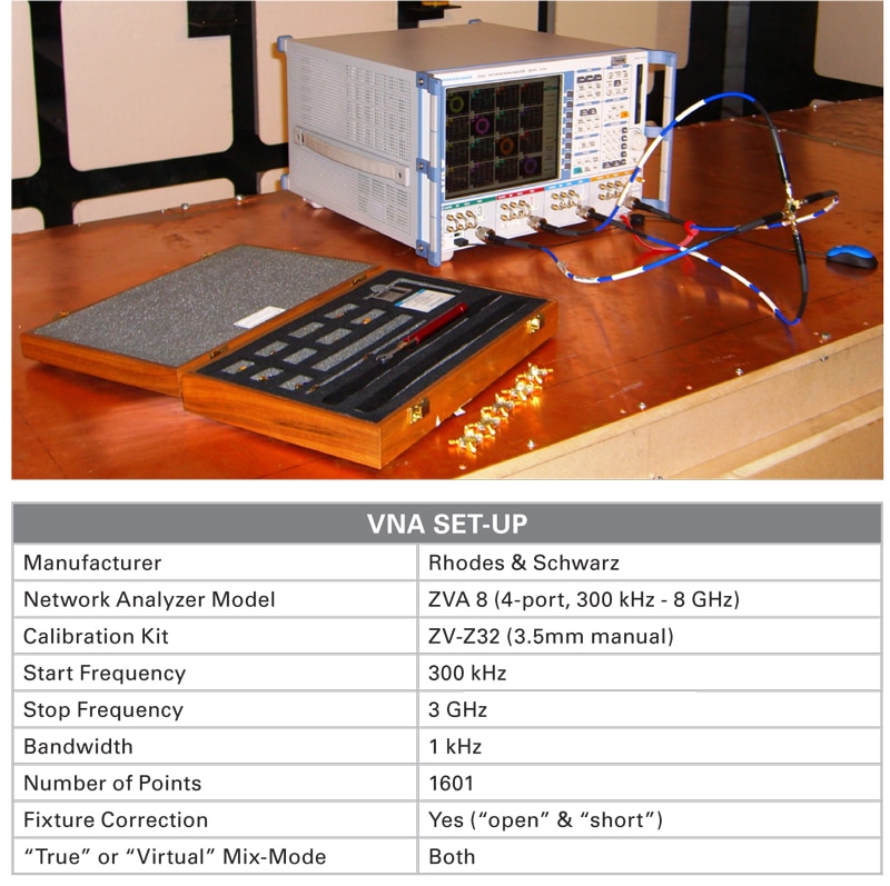
Figure 8 depicts the setup using a Rhode & Schwarz ZVA 8 Network Analyzer. The analyzer allows for both “virtual” and “true” mix mode measurements.
RESULTS AND CONCLUSIONS
Figure 10 and Figure 11 below are the measured results of the 2 different automotive CANBus CMCs. The two samples are from different manufacturers and are specified for use by an automotive OEMs. From the data, one can see a noticeable difference in the “virtual” and “true” measurements especially in the CD and DC measurements. As described above, the “virtual” measurement transmits a signal one-port at a time, and then looks at the responses of the four-ports. The “virtual” mix-mode measurement is then calculated using software. A “true” measurement transmits a signal on two ports simultaneously. The responses of the four ports are then measured. The “true” mix-mode measurement is an actual measurement. In the case of a CMC, both lines are wound around a ferrous material so the resulting H-Fields cancel and block unwanted CM content from passing. To take full advantage of the H-Field cancellation, both lines of the CMC must be activated. In the “virtual” measurement, only one line of the CMC is activated at a time; whereas, the “true” measurement activates both lines of the CMC resulting in a more realistic response.

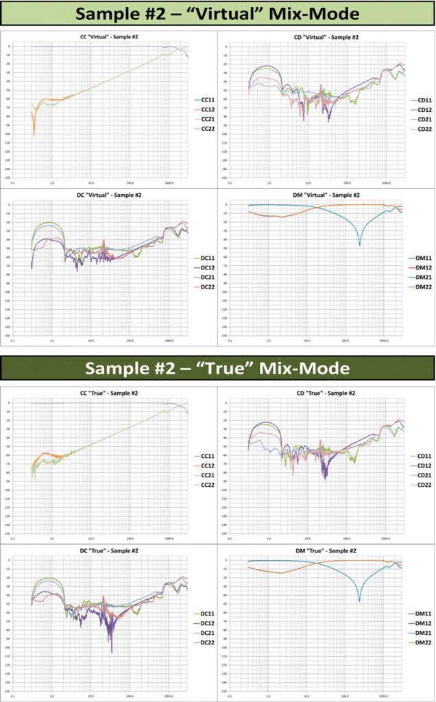
Additionally, DM measurements exhibit a significant amount of parasitic capacitance. The response is similar to that which might be obtained by measuring a parallel capacitor with two-ports of a network analyzer. Below are calculated values of the parasitic capacitance shown in the DM measurement in Figure 10 and Figure 11. Note that capacitance values far exceed the typical 56-100 pF allowed by automotive OEMs at each CANbus node (Figure 9).

Looking at line-to-line balance, CD and DC conversion modes would have a zero dB value if no conversion had occurred.[3] Since conversion did occur, it is interesting to see how well the forward and reverse transmission measurements (CD12 & CD21 and DC12 & DC21) tracked for the two samples. As shown in the Figures 10 and 11, as much as 30dB of separation occurred between 10 MHz and 100 MHz for the transmission measurements of both samples.
In conclusion, the test methodology described in this article shows promise in evaluating dual-line EMI filters and provides insight into details that are not fully specified by EMI component manufacturers. Results are consistent with previously published measurement methods of evaluating a dual-line EMI filter. [4, 5] Future work might concentrate on developing a standard methodology to perform dual-line EMI filter evaluations.
ACKNOWLEDGEMENTS
We would like to thank Rhode & Schwarz and Agilent for equipment and technical support as well as AOAMR-DT Labs in Farmington Hills, MI. Additionally we would like to thank the following individuals for their support and help: John Yochum, Elizabeth Wittwer, Tony Seccia, Tom Holmes, Mohammad Shamsher, Patrick Means, and Jeffery Markham.
References:
[1] Agilent Technologies, “Multiport & Balanced Device Measurement Application Note Series: Concepts in Balanced Device Measurements,” Application Note 1373-2.
[2] Agilent Technologies, “Agilent De-embedding and Embedding S-Parameter Networks Using a Vector Network Analyzer,” Application Note 1364-1.
[3] Greg Amorese and David Ballo, “RF Balanced Device Characterization: Part 1 & Part 2,” Agilent Technologies, Part 1 – January 14, 2003 and Part 2 – January 23, 2003.
[4] James P. Muccioli and Anthony A. Anthony, “Dynamic Testing of a Dual Line Filter for Common and Differential Mode Attenuation Using a Spectrum Analyzer,” Interference Technology EMC Directory and Design Guide, April 2000.
[5] I. A. Maio, P. Savi, I. S. Stievano, and F. G. Canavero, “Augmented Models of High Frequency Transformers for SMPS,” Proceedings, 20th International Zurich Symposium on EMC, February 2009.
James P. Muccioli has been an EMC consultant with Jastech EMC Consulting LLC for over 20 years. Additionally he has worked for X2Y Attenuators, DaimlerChrysler, and United Technologies as an EMC expert and system engineer. He has taught EMC undergraduate courses and continuing education seminars at Lawrence Technological University and at the University of Michigan. He is an iNARTE certified EMC and ESD engineer and a member of SAE J-1113, J-551 and chairman of IC EMC Task Force. He was named an IEEE Fellow in 1998 for contributions to integrated circuit design practices to minimize electromagnetic interference and has served on the IEEE EMC Society Board of Directors (1993–1998 and 2001–2003).
Dale Sanders is an independent EMC consultant with Jastech EMC Consulting LLC. He serviced in the U. S. Marine Corps from 1993 to 1998. He has a BSEE from the University of Michigan, where he currently is a guest lecturer and works with the ECE Department to develop EMC course criteria and lab experiments. His experience includes IC design and layout, component testing, and EMI filter design with Xilinx Inc & X2Y Attenuators LLC. He is an active member of the IEEE EMC Society, SAE EMC Committees, and IC EMC Task Force. He has authored numerous EMC technical papers, as well as numerous application notes on EMI filter products.


