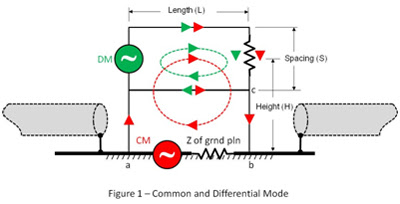
Apparently, I didn’t throw enough words at the CM/DM problem in the last several posts so I’m going to add to it, but from a slightly different perspective. It’s either that or hide my email address. I’ll do DM this time, CM next time.
We’ve been discussing loops all along. If there’s current, there is a loop somewhere. Finding it may be a problem. DM loops are bad, but CM loops are worse. Sometimes the loop is so poorly defined or obscure that it is difficult to comprehend that there really is a loop and that it is returning current to a source. This is especially true with logic traces, wires, and cables because they all appear to be single ended.
Dr. Howard Johnson said in the article, “Why Digital Engineers Don’t Believe in EMC”, IEEE EMC Society Newsletter, Spring 1998, that many digital engineers don’t believe current flows in loops and, because of this, think signal return paths are irrelevant.
The return paths are very relevant! If the circuits that are being driven do not have a stable, well-defined return path, the current will return to its source the best way it can. Unfortunately, this may be the worst way for EMC. Generally, these strange return paths are unacceptable. They increase radiated emissions from the circuit, capacitive and inductive cross-coupling (AKA crosstalk) between circuits, and the susceptibility of circuits that are closely coupled to the undefined path . . . most of the time by wires and cables.
Controlling the circuit loop area (A = conductor length L x spacing S) is probably the most important element in meeting EMC requirements. As the loop area increases, the levels of generated or intercepted energy will increase. Therefore, keep the loop areas as small as possible, especially those operating at a high frequency/speed. Unfortunately, since the conductors are the principle determinant of loop area, there is a limit on how small we can make the radiated emissions or susceptibility loop because of physical constraints. Loops can’t be any smaller than the area required by component placement. On a PCB, the trace loops will be a lot smaller than the loops formed by wiring and cable placement between racks located on separate floors within a building.
Unless the circuit loop is completely isolated from all other conductive surfaces, each loop will have two coupling modes: the green differential mode (DM) and the red common mode (CM). DM, typically a differential pair over a ground plane in a high-speed system, and CM, where some synchronous current from both the signal and its associated return lead, are conducted via a common reference surface, are illustrated in Figure 1.
The electric field (E) radiation created by DM current circulating around a small, nonresonant loop oriented at angle (θ) is given by John Kraus as:
E = 120 π2 A I sin (θ) / (λ2 r)
By orienting the loop for maximum emissions, something that is done during the EMC measurements by rotating the unit, raising and lowering the antenna, and changing the antenna polarization angle, we maximize the signal making sin (θ) = 1. Converting to frequency instead of wavelength, F(MHz) * λ (m) = 300 m/μs the equation can be simplified as:
E = 1.32 A I F2 / r
Where:
E (max) = µV/meter
A = radiating loop area (sq cm), 0.1<(l/w)<10 br="br">I = drive current (amps)
F = emissions frequency (MHz)
r = measurement distance (meters)
Kraus indicates that for frequencies below resonance this equation is accurate to within 1% for loops up to 10 x 10 inches. This makes it ideal for PCB design.
However, it certainly is usable for any loop current at frequencies below loop resonance where the length to width ratio is <10 font="font" size="3">.
– Ron Brewer


