This is post 2 of AR’s blog series “Specifying RF/Microwave Power Amplifiers for EMC Testing.” The full series can be viewed here.
INTRODUCTION
How much input power is required to achieve full rated output power is a common concern when choosing an amplifier. Amplifier manufacturers have specified an input of 1 milliwatt. (Note that this is not the case for every manufacturer – be sure to verify). While the rated input power is defined as 1 milliwatt, most amplifiers provide rated output power with less than 1 milliwatt input. This is because the specified value will often have built-in conservatism.
AR Amplifier typical input levels:
Signal Generator: 1 milliwatt which is equivalent to 0 dBm
Function Generator: 1 milliwatt or 224 millivolts into 50 Ω
Max input before damaging amplifier: +13 dBm or 20 milliwatts (20 times more power than 0 dBm)
Note: Pay close attention to an amplifier’s maximum input. It varies by vendor and possibly by model family.
The input signal strength has a profound effect on the amplified output signal. It determines the operating region and thus, the degree to which the amplifier output is compressed. Ideally, an amplifier will simply amplify the input signal without adding any additional signals or artifacts. Unless operated in the extreme linear region, amplifiers will distort the input to some degree. The extent to which the amplifier affects the input signal is a function of the output compression. The higher the amplitude of the input signal, the risk of higher the output compression increases. At the 1dB compression point, there may be a slight flattening at the top and bottom of a CW sine wave signal. As the amplifier is driven further into saturation, additional distortion will become apparent and eventually, the CW input signal will approach a square wave output (See Figure 5). The 1 dB and 3 dB compression points are further shown in Figure 6.


Figure 5: Example of Amplifier Saturation

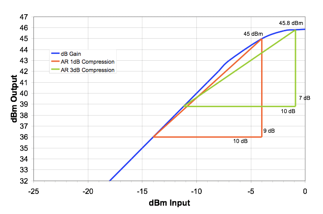
Figure 6: Linearity Characteristics
Distortion creates new unwanted signals at frequencies not present at the input of the amplifier, as observed in the frequency domain with a spectrum analyzer. Figure 7 shows the effect of driving a TWTA amplifier into saturation. This figure shows the harmonic having only a slightly lower amplitude compared to the fundamental signal. This situation causes unnecessary problems for the test engineer. Under this scenario, if the EUT fails during radiated immunity testing, the test engineer will not know if the cause of the failure were due to the fundamental or the harmonic. To further complicate matters, if additional harmonics have high amplitudes the test engineer must evaluate all harmonics to determine the cause of the failure. It is also possible that neither the fundamental or a single harmonic causes a failure, but a combination of the fundamental and harmonic(s). Measuring the amplifier output power or the generated field are further complicated since most commonly used power meters and field probes are themselves wideband measurement devices and will display the total energy across the entire band, fundamental, harmonics, and spurious. It should be noted that AR’s solid-state Class A amplifiers produce far less harmonics than TWTAs, they are rated for -20 dBc at the 1 dB compression point. This greatly reduces the EUT’s exposure to unwanted RF energy during radiated and conducted susceptibility testing.

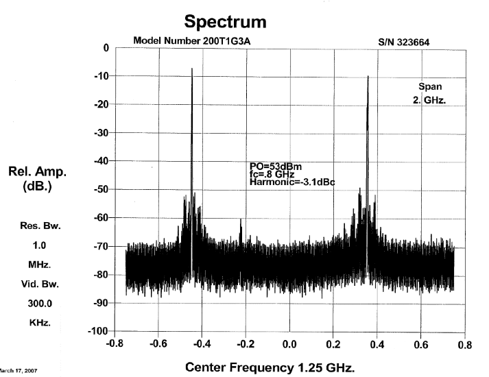
Figure 7: Image of the Fundamental Signal and harmonic
For additional information on effects of input power see: Application Note #45 Input Power Requirements for AR RF/Microwave Instrumentation’s Amplifiers.
TYPES OF AMPLIFIERS
In general EMC amplifiers range in type, such as: Solid State, TWTA, CW, Pulse, and their class of operation – Class A and Class AB.
CLASS A CLASS AB TYPE AMPLIFIERS
Class A and Class AB amplifiers have their strengths and weaknesses. Class A amplifiers are the most robust. They provide the highest levels of mismatch tolerance which is needed when significant RF levels reflect into the amplifier. This is a common effect with many EMC antennas and other transducers. Additionally, linearity and harmonic distortion are much better with Class A amplifiers compared to other amplifier classes.
Class AB amplifiers have their own benefits. Generally, the cost of the amplifier is less than Class A amplifiers. The physical size of these amplifiers is also generally smaller. These amplifiers are much better suited for use with matched loads. See Application Note 27A.
Shown in Table 2 is a summary of the differences between Class A, and Class AB amplifiers.
Table 2: Comparison of Amplifier Class of Operation
| Characteristic | Class A Amplifier | Class AB Amplifier |
| Output distortion | Low distortion, highest Linearity | Higher distortion, poor Linearity than Class A |
| Bias Scheme | Output current flows for 360° of the input signal | Output current flows somewhere between 180 and 360° of the input |
| Ruggedness | Amplifier will safely operate without damage regardless of load mismatch | Output limits are generally used to protect the amplifier when operated beyond a stated level of mismatch |
| AC power to RF power efficiency | Less efficient | More efficient than Class A amplifiers |
| Construction | More components required to share the heat load | Less components required to share the heat load than Class A amplifiers |
| Size/Weight | Larger/Heavier | Smaller/Lighter than Class A |
| Cost | Higher than Class AB | Lower than Class A |
A summary of mismatch performance for typical Class A and AB amplifiers is shown in Figure 8. The 100 Watt curve is representative of most AR amplifiers below 500 watts. It is clearly seen that the amplifier delivers a Minimum Available Power (MAP) of 100 watts irrespective of the load VSWR, including output load opens and shorts. As output power increases it becomes increasingly difficult to absorb 100% of the reflected power uniformly. Hot spots at these elevated power levels can cause damage or at least affect reliability. Nevertheless, AR high-power amplifiers continue to offer 100% mismatch tolerance up to a load VSWR of 6:1 (lower-power amplifiers deliver full power regardless of mismatch). Once this level is reached, the output power is limited to 50% of rated power. For example, the AR model 2500A225A amplifier will provide a MAP of 2500W up to a load VSWR of 6:1. At this point, approximately 1250 watts is reflected. From this point on, as load VSWR increases the output power is gradually reduced until it reaches 1250 watts for an infinite load VSWR.
In practice, the AR’s conservative VSWR compromise of 6:1 works well in that the VSWR of EMC antennas and transducers is often held to this value or better. If it strays beyond, rest assured your AR amplifier has sensed the increase and has implemented sufficient limiting to protect the amplifier from any damage. Based on the above, mismatch tolerance can make the difference between meeting or failing the required power or field levels. As a result, mismatch tolerance is an important specification to consider when comparing offerings from different manufacturers, and where some manufacturers with use terms such as typical, or protection to confuse the issue.

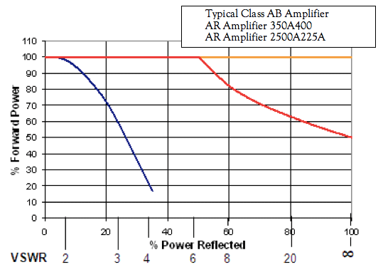
Figure 8: Minimum Available Power
TWTA AMPLIFIERS
For years, when discussing microwave, high field-strength electromagnetic compatibility (EMC) radiated susceptibility testing, Traveling Wave Tube Amplifiers (TWTAs) were the only choice for wide frequency coverage, and power. TWTAs are lower cost solutions, in most cases, but do have drawbacks. Their unique properties allow them to be used in a pulsed mode, that can lower the total required average power, but maximize their peak power and thus reducing the cost further. However, TWTAs produce high harmonics, have a greater noise floor, longer purchase lead times, longer repair times, and lower reliability than solid-state amplifiers. Some advanced TWTAs combine multiple tubes together to reduce harmonic content and increase total power. Another solution to reduce harmonics is to use filters on the amplifier output. It’s important to remember that there are always losses associated with filters that must be considered for amplifier power sizing. The VSWR associated with the filters is another consideration, which can cause amplifier foldback.
SOLID STATE PULSE AMPLIFIER
The difficulties associated with pulse TWTAs are mitigated with a new, very attractive alternative. Solid state pulse amplifiers now offer high-power RF levels that rival those of TWTAs. AR’s SP-series amplifiers include various frequency ranges and output power levels to meet several standards and user requirements. These solid-state pulse amplifiers offer higher reliability, better mismatch tolerance, much better harmonic distortion, and better MTBF (Mean Time Between Failure) than TWTAs.
DUAL BAND AMPLIFIERS
If a single band amplifier is not available over a desired frequency band, a dual-band amplifier may be an attractive solution. A dual band amplifier consists of two amplifiers that are combined into one “box” with a single I/O interface, RF input and output, and two bandwidths equivalent to the two amplifiers it replaced. This approach simplifies the test setup.
While on the surface the system seems simplified, a closer look within the “box” reveals a different story. While the two amplifier modules in a dual-band amplifier may share a common power supply, the overall system is complicated by the fact that it now consists of not one, but two complex amplifier modules.
Furthermore, additional RF switching, cabling, and connectors are required which will adversely affect the RF output of both amplifiers. The additional components add insertion loss that may not present a problem at lower frequencies but can account for significant losses at higher frequencies. Also, simultaneous signal generation across the entire band is not possible, due to the required switching from one frequency band to the other. So, as you can see there are pros and cons to dual-band amplifiers.
Figure 10 and Figure 11 show the schematic differences between a single band and dual band amplifier, respectively.

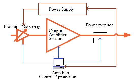
Figure 10: Basic Diagram of a Single-Band Amplifier

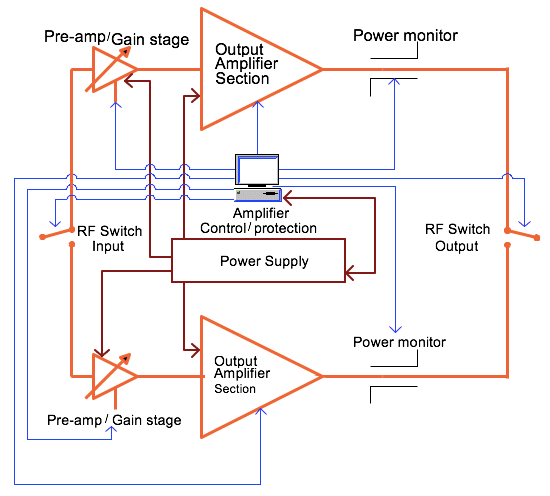
Figure 11: Basic diagram of a Dual-Band Amplifier
AMPLIFIER ACCESSORIES
An often-overlooked important part of an EMC test setup are the accessories. The cost and time associated with EMC testing warrants the use of high-quality accessories.
AR offers accessories with an experienced sales and engineering organization available to provide customers the best solution. Figure 12 and Figure 13 are examples of accessories used in radiated and conducted RF immunity test setups, respectively.

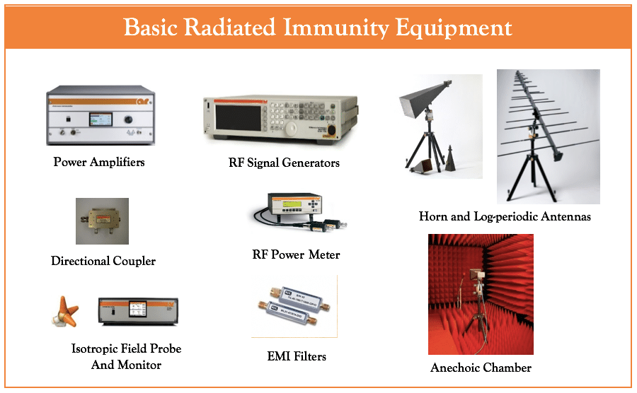
Figure 12: Components Used In a Typical Radiated Immunity Test Setup

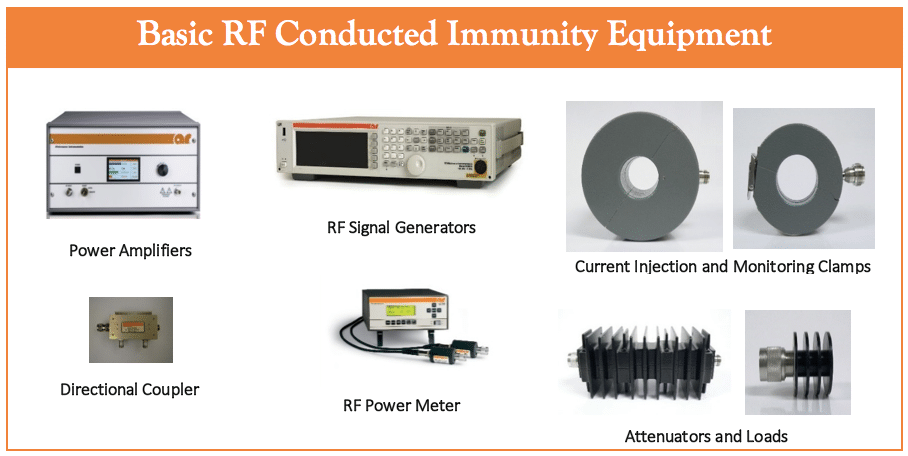
Figure 13: Components Used In a Typical Conducted Immunity Test Setup
Additional Reading: Amplifier Selection Tips
Next Topic:
Specifying RF/Microwave Power Amplifiers for EMC Testing – HIRF & High-Frequency Field Generating Systems
