NOTE: This article has been translated from German into English. It can be found in its original language in the 2014 EMC Europe Guide.
Tobias Hofer
EMC Consultant
HSI Elektonik AG
Switching power supplies can be found in nearly all electronic devices. The efficiency should be as high as possible. The no load condition should be in the milliwatt range. In contrast to that, the overall product cost should be as low as possible. “Time to market” for new developments is becoming increasingly important. A product can only enter the market if it complies with the standards.
Often the EMC filter is a crucial part for an optimal solution. The right EMC filter topology can save a lot of time during certification and EMC optimization of the product. Furthermore an optimal EMC filter will reduce the production cost and the volume of the product.
The following technical article gives an insight into the field of EMC filter design. We will show why it is so important to consider the parasitic of the filter elements, and how a practical simulation approach can speed up the design process.
The success of a product depends on, how quickly it is available in the market. The certification of the product is often a time consuming part. It is getting worse if we are failing during the certification process. The result could be a redesign of the whole product which will certainly increase the development cost. The market entry of the product is delayed which causes even more cost.
If we are looking at the EMC emissions of a power supply we are having two kinds of emissions. Conducted emission, mostly measured in the frequency range between several kHz and 30MHz. The radiated emissions are in the range between 30MHz and several GHz. To reduce the conducted emission one is using an EMC line filter. The EMC line filter (i.e. in switching power supply) could be a big part of the whole product. Also a “normal” condition during development is that that we always have less time. The product should be finished even before the development has started. Due to the lacking of time, the proposed solution is probably not the optimal solution. The result is an often over-sized filter that causes unnecessary costs. Depending on the design, the costs of materials can rise up to 15% of the whole product price. An often-used EMC filter design technique is the “cut and try” method. That is, we are replacing filter elements like inductors and capacitors. Soldering them together until the measured interference is within the limits. Often one cannot understand what impact that changes had afterwards.
In the end there is a solution, but are we having the best solution with this approach?
Interference Type: Common Mode or Differential Mode
For an optimal EMC filter design, it`s important to know the type of interference. We should also know in which frequency range the type of interference is dominant. With the conducted emission we can distinguish between differential mode (DM) and common mode noise. The differential mode noise is often dominant in the low frequency range up to 1 MHz. In switching power supplies the source of this type of noise is the voltage drop across the ESR of the dc-bus capacitor. The voltage drop is caused by the ripple current. (i.e. from the active PFC). Common mode interference (CM) acts between 1MHz over a hundred megahertz. In this frequency range parasitic effects and coupling paths must be considered. The type of noise has a major impact on the design of the EMC filter. If both factors are known and if we know the coupling paths, we can start with the filter design.
Capacitive Chokes and Inductive Capacitors
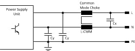
The most common filter structure for an EMC filter is the LC topology, designed to suppress CMM and DM noise. The right choice of the inductance plays an important role. One important point to consider is the frequency behavior of the common mode inductor. In the following we are going to design a LC filter. Figure 1 shows the topology.


EMC Filter Design Based on Measured Values
Normally we proceed in optimizing an EMC filter as follows: We are measuring the noise spectrum. We should also try to differentiate between common mode noise and differential mode noise. If we know the amplitude of the noise and if we know about the limit, we can calculate what attenuation is needed in a certain frequency range to comply with the limits. The calculation for the needed attenua-tion can be done in several ways.
One possibility is to use a paper and pen. Then we can do our calculation based on theoretical values of the inductance and capacitance. As we have shown earlier, this is not the best way, particularly in the high frequency range because of the parasitic elements in filter elements. Another solution is to use a spice simulator. For a meaningful simulation we must derive the equivalent circuits of the single filter elements which consider all parasitic elements. Depending on the needed accuracy and number of elements, this can be a time consuming procedure.
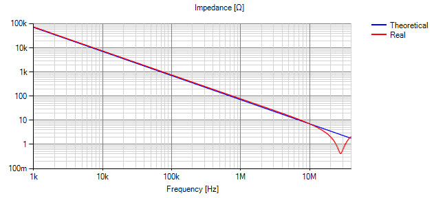
Another solution is to design and simulate the filter directly with the measured impedance curve of the filter elements. As we can see from figure 2 and 3 the impedance curve includes the parasitic elements. If we manage to work directly with the impedance curve of the real filter elements we get a very accurate simulation of our filter.
What do we need for this approach?
First we need a vector network analyzer (VNA) to measure the impedance and phase curve of the filter elements over the desired frequency range. For the simulation shown in this article we have used a VNA with an external impedance adapter to measure the filter elements. Figure 4 show such a setup for measuring the impedance over the entire frequency range.


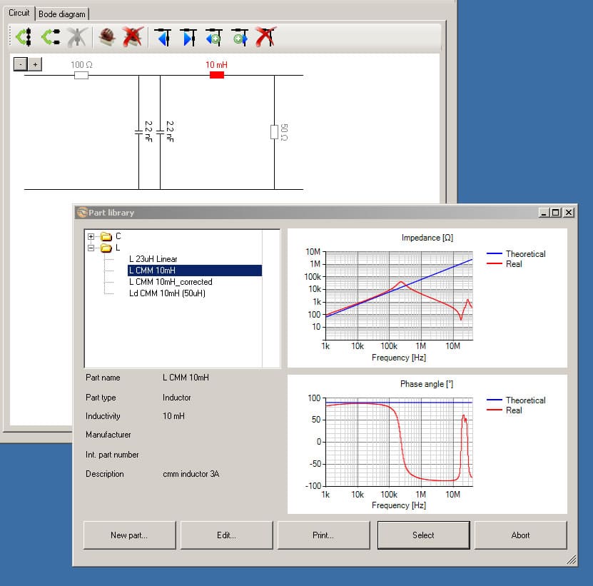
In figure 5 we can see that there is a window to draw the schematic of the filter. Behind the filter ele-ment (i.e. the red marked inductor in figure 5) there is not a spice model. Instead of that we are using directly the complex impedance curve of the elements. This approach has also the advantage that it is very fast. With the VNA we can measure all elements we would like to use ore we are having in our shelf for filter design. Directly after we have the measured values in our library we can simulate the new filter including the parasitic elements.
Optimization: Filter Performance is Worse Than Expected
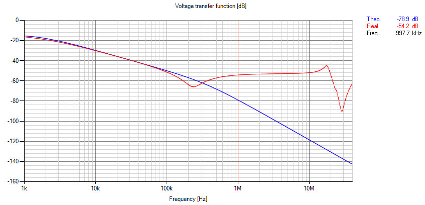
In our example we are designing a LC common mode filter. As we know, common mode noise is mostly dominant between 1MHz and 30MHz for conducted emissions. If we now simulate the filter proposed in figure 1, based on the measured frequency behaviour of the inductor and the capacitors we get the following result:

Figure 4 shows the simulated common mode frequency response with the ideal components (blue). The red trace shows the simulated frequency response based on the measured filter elements. For the simulation in figure 6 we assumed an output impedance of the power supply of 100 ohms. The impedance on the power line side was considered with 25 ohms. In figure 4 we see the first resonant frequency at 200 kHz, which is based on the resonant frequency of the common mode inductor (see figure 2). At 20 MHz we can see a second resonant frequency, which is the result of the stray inductance of the common mode inductor. At 30 MHz we see the resonant frequency of the CY Y-capacitors.
The red cursor at 1 MHz shows us a difference of more than 20 dB between the theoretical attenuation of the filter and the result based on the real values. This means that the designed filter is having 10 times less effect in attenuating the noise than expected! Other effects that reduce the filter performance in practice are not yet included!
This example shows as that it is insufficient just to design using theoretical values.
Practice: A Story from the EMC Lab
In the past, it happened a lot to us. We are working on a prototype, looking for a solution to reduce the conducted or radiated emissions. We are replacing a 10-mH choke with a 15-mH choke, for example. We have in mind that 15mH are better than 10mH. The result is that the interference is reduced in one frequency range and in another, the interference increases! The RF behaviour of the real components could have been the reason. The same size of a CMM choke with more inductance has often a higher parasitic capacitance, due to the increased windings. The resonant frequency is therefore even at lower frequencies. With the presented approach, one can consider this effects without spending too much time with soldering.
CONCLUSION
To find the optimal solution in the shortest possible time, a structured approach is of most interest. First of all, we should know the type of interference and the frequency range of interest. For interfer-ences above 1 MHz the RF behaviour of the filter elements needs to be considered. A simulation approach which considers the parasitic and the frequency behaviour of the filter elements led to a more optimized solution. The development time and the product price can be reduced. Also this simulation approach can lead to a better understanding how the EMC filter works.
REFERENCES
[1] Simulation and measurement are done with the EFsyn software
ABOUT THE AUTHOR
Tobias Hofer studied electrical engineering at the ZBW St.Gallen. He has begun a division of EMC Consulting, HSI Elektonik AG. Email him at tobias.hofer@hsi-ag.ch or visit www.hsi-ag.ch.


