IC immunity tests under the influence of ESD
Sven Konig
Nowadays, electronic devices have to meet the highest standards in terms of ESD immunity. “According to estimates of TÜV NORD, the manufacturing industry incurs costs amounting to millions of euros every year due to electrostatic discharges. ESD effects lead to circuit failures which in turn bring a vehicle, a process or a production line to a halt.”[1]. An electronic system must be able to function reliably and without failure even under the severest conditions.
But at best an electronic system is only as good as its individual components, which must consequently meet these high demands too. A special point of interest is integrated circuits (ICs), which hardly any of today’s electronic systems can do without. But which tests are available in practice to evaluate ICs in terms of their ESD immunity and how are these tests carried out?
Metallic housings and complex EMC measures such as ground layers, filters, etc. are often used to make modules or devices immune to ESD. These methods are very expensive and require a great deal of development work. Conventional EMC measures are usually only used for the prototype or at a very late development stage of the module or device, and even then, only if the compliance test has shown that the device’s immunity is inadequate. These measures are taken to ensure the device’s functionality. A much better solution, however, would be to subject the components intended for use such as ICs, connectors, etc. to comprehensive EMC analyses [2] and especially to an ESD test right from the beginning even before the electronic development process starts. This would allow the developer or designer to make plans on how and where to use the components on the basis of their robustness and help him save time and cut development costs.
There are usually two different approaches that can be chosen in practice to ensure a module’s or device’s EMC.
In the first approach, the device is developed up to the initial sample or prototype. At this development stage the device is subject to an EMC compliance test where the EMC requirements are defined for the complete system. Potential weak points such as inadequately dimensioned connectors or sensitive ICs are only discovered in this compliance test and it will not be easy to modify them at this stage. The entire device or the module will be unable to achieve the defined EMC objectives so that comprehensive redesign work will be necessary, which in turn will entail a loss in development time and additional EMC measures.
In the second approach, which is better, a separate EMC test is carried out for each of the planned components before the development process starts. This helps the developer determine their EMC parameters and assess if they suit the actual EMC demands of the entire system. It is thus possible to select appropriate components for a robust electronic design when the development is being planned.
ICs are particularly important for the EMC immunity of modules and devices. The IC’s are becoming smaller and smaller and their clock rates faster and faster. The operating voltages as well as the associated operating points are being constantly reduced for energy efficiency reasons. This often makes ICs the weak points of the entire system and it is thus particularly important for them to satisfy the defined EMC requirements. For this reason EMC tests have to be carried out on ICs to ensure the functionality of the entire system.
The test procedures for ICs must be based on the compliance tests for devices. But conventional compliance tests cannot be used directly for ICs since the disturbances defined in the standard do not become effective on the IC during a compliance test on the module. The standard disturbance that is coupled into the device with a disturbance generator from outside subjects the IC and its line networks to magnetic and electrical fields. Due to this effect, namely magnetic and electrical coupling, the disturbances at the IC differ from the standard disturbances in terms of form, amplitude and mode of action. IC test procedures thus have to be redefined as separate test procedures.
Apart from the desired standard pulse, parasitic fields are similarly generated directly by the generator which may also interfere with the device as a whole or its individual parts[3]. These unwanted electrical and magnetic fields essentially depend on the type and position of the ESD generator. This may lead to a great deal of inaccuracy in device tests. Even the direct ESD tests on individual IC pins carried out by some IC manufacturers are thus inaccurate and cannot be reproduced.
Disturbances therefore have to be defined at the circuit on the basis of magnetic and electrical coupling. In the event of magnetic interference, the disturbance current generates a corresponding magnetic field in the device. A disturbance voltage can be induced in existing loops (e.g. line networks). This disturbance pulse drops on high-impedance IC inputs and interferes with these. Furthermore, the disturbance can also affect other areas within the IC such as PLL, core, etc. The supply system, low-impedance signals as well as lines that are capacitively connected to the ground or Vcc, for example, are critical lines when it comes to interference through magnetic fields.
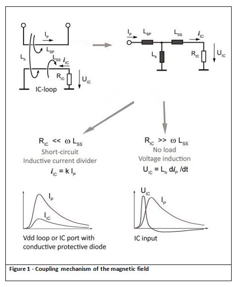
The magnetic coupling effect can be compared to a transformer (Figure 1). Interference with the IC’s low-impedance Vdd loops results in an inductive current divider. The disturbance current generated by the disturbance generator is transferred to the IC’s line networks. Interference with IC inputs that are connected at low impedance leads to the differentiation of the disturbance pulse if a magnetic field is applied. The induced voltages have much faster rise times and are shorter than the actual disturbance generated by the ESD generator. Today’s circuits are fast enough to evaluate these differentiated disturbances (< 1 ns) and to be affected by them.
It is mainly lines with high impedance that are sensitive to electrical interference. The voltage difference between the circuit and its environment such as metal parts, ESD generator, etc. generates an electrical field that may affect the signals or the circuit. The resulting voltage pulse may lead to an interference with the IC depending on its sensitivity. Reset, clock, quartz, test pins or high-impedance measurement inputs of A/D converters, for example, are critical pins or lines.
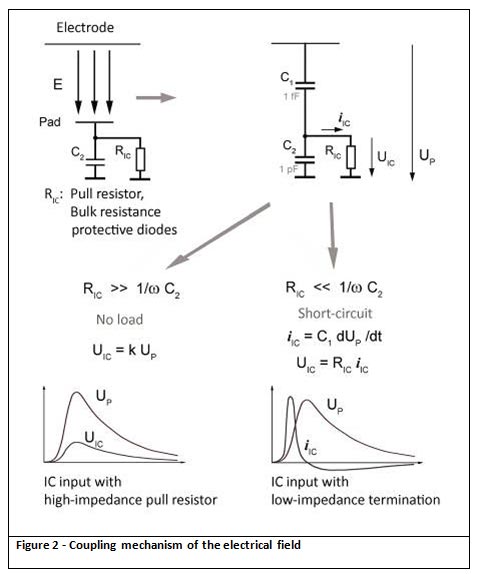
The capacitance between the IC’s line networks and its environment is the quantity that is decisive for the coupling mechanism of the electrical field (Figure 2). The disturbance is also differentiated if an IC input that is wired at low impedance is subject to capacitive interference. The disturbance pulse is transmitted directly via the capacitive voltage divider if the lines are connected at high impedance. The effects on the IC are ultimately similar to those caused by magnetic coupling.
Today’s manufacturers usually test the resistibility of their ICs. These tests (e.g. HBM; MM; HMM) only ensure the IC’s resistibility during production, for example. They have nothing to do with how an IC can be interfered with in its respective field of use. Tests that are based on standard burst and ESD tests are nowadays used to ensure an IC’s trouble-free operation. The transient injection method (IEC-62250-3) requires that disturbance pulses from the standard burst generator are applied directly to the IC pins. This generator, however, has no matched line termination and the measurement set-up is electrically long resulting in undefined disturbances. Instead of using the disturbance current and/or disturbance voltage directly at the pin, the no-load voltage at the generator is used to evaluate the IC’s immunity. The disadvantage of this method is that it allows no conclusions on the IC’s sensitivity to electrical or magnetic fields. The powered ESD susceptibility test (also HMM) requires that the ESD pulse is applied directly to the IC pin. This disturbance will not occur in this way at the IC in practice. Furthermore, unwanted electrical and magnetic disturbance fields, are generated at the ESD generator which will also affect the IC under test. This makes the tests hard, if not impossible to reproduce.
Useful test procedures must simulate the physical principles of action in the device. A very low-impedance source (R<<50 Ohm) is required to simulate magnetic coupling into the IC pin. This allows the generation of a disturbance as occurs in IC use through voltage induction in the IC or at the line networks (Figure 3). A disturbance generator with a very high impedance is required to simulate electrical coupling (R>>50 Ohm). In conjunction with a very low coupling capacitance, this allows the simulation of electrical interference (Figure 4).
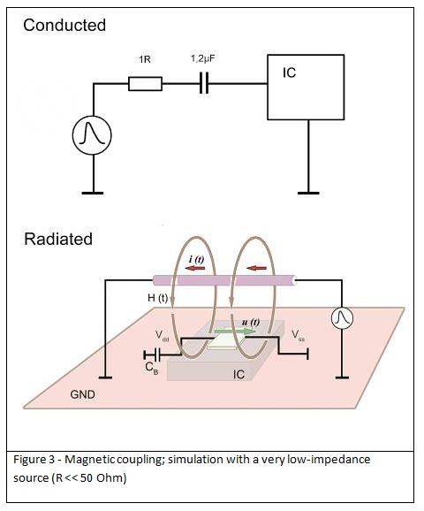
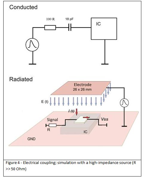
The IC test system allows the user to perform different test procedures on the circuits without interaction and in a reproducible way.
The IC is mounted on a test board and connected to all necessary and/or wanted signals and a power supply. This test board enables an EMC compliant connection of the device under test and contains all necessary filter elements to ensure that the IC and its environment are decoupled. The test board is connected to the connection board. The connection board is a unit that is used to control and monitor the device under test (IC). The test board and the connection board are located in the ground plane. The ground plane is the reference ground for the tests. The device under test and the corresponding test systems (probes) can thus be properly connected under RF conditions and the measurement set-up is confined to a small space. The probes are suitable to perform both emission measurements and immunity tests (Figure 5). They are placed on the ground plane and connected to this at low impedance. The probe allows the user to contact any pin flexibly and directly. The complete measurement system is contained in the probe and does not have to be integrated in the layout of the test board.
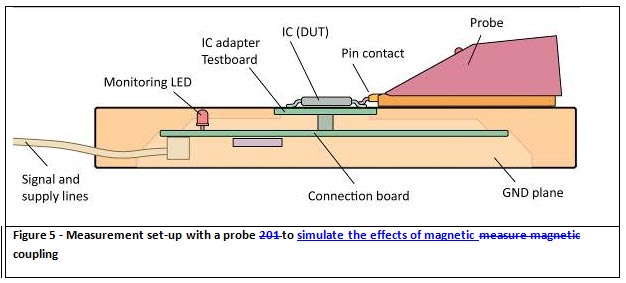
Different probes can be used to simulate the ESD principles of action mentioned in the first part of this article. A very low-impedance pulse generator is integrated in the current probes to simulate the effects of magnetic interference that affect the IC in practical use under the influence of ESD. The interference mechanisms caused by electrical fields can be simulated with the voltage probes. These have high impedance and a very low coupling capacitance. The test system enables the developer to contact an individual pin and determine the different electrical and magnetic interference levels of a pin through an automatic test procedure if necessary. Apart from conducted IC test methods, a variety of systems for radiated measurements (RF, ESD, Burst) are available.
The IC test system has the following benefits for the users:
- the EMC parameters of individual components can be compared directly
- components can be selected for specific layouts
- the immunity behaviour of components can be predicted
Similarly, the IC manufacturers can benefit from testing their circuits with the IC test system:
- the EMC parameters of existing ICs can be verified
- causes of disturbances can be clarified
- IC optimisation processes can be carried out with the IC test system in an efficient and expedient way
The IC test system is suitable to perform all IC measurements/tests (compliance measurements as well as measurements during development) and to determine all relevant EMC parameters of ICs.
Further reading:
“Guideline IC EFT”, Langer EMV-Technik GmbH (to get the document, please contact k.langer@langer-emv.de)
Information to be noted by the editorial office:
Should you change the manuscript, we would kindly ask you to send a galley proof to k.langer@langer-emv.de so that the author can correct this before the contribution is printed.
We would like to point out that we transfer to your editorial office the non-exclusive right of use (section 31 subsection 2 of the German Copyright Act) to the contribution (text, graphics, photos) for the publication and distribution (print + online, unrestricted in terms of time, place and content, no resell, no forwarding) in the English and Chinese language, taking your wish to publish it first into due account. We reserve the right to publish the author’s version in full or in part in the aforementioned languages also ourselves one year after the date of publication (print).
Langer EMV-Technik GmbH reserves the right to use the author’s version of the contribution, or also your contribution with a respective link, for the Internet presentation of Langer EMV-Technik/Specialist articles after a waiting period of 30 days after the external date of publication. Langer EMV-Technik GmbH also reserves the unrestricted right to publish the contribution in other languages.
Should you be able to make a pdf file or an Internet link available to us at a later date, we would appreciate receiving notification from you to this effect.
[1] TÜV Nord in ELEKTRONIKPRAXIS no. 4, 20.02.2014, page 23
[2] Dipl. Ing. Lars Gläßer; Measurement of pulse immunity of microprocessors and microcontrollers; ECE; 09/2012
[3] Dipl. Ing. Gunter Langer, EMC Properties of ESD Generators, InCompliance/annual guide, 05/2014


