Author
Bruce E. Touzel, Cisco Systems, Inc.
The Opportunity
More and more, 3G wireless modems are finding their way into places other than your typical mobile phones and laptops for internet connection. A term called M2M (machine-to-machine) is defining the new 3G communications link between machines for telemetry and other industrial & commercial purposes such as routing of IP traffic. Considered to be one of the upcoming market transitions, 3G wireless connection for an M2M configuration presents cost effective opportunities, continuous communications at broadband data rates, with wide spread service coverage, innovative applications, lower power consumption, more compact sized enclosures, reduced monthly air time charges, in just about any location. Traditionally, telemetry involved remote monitoring of industrial locations such as power, water, and gas utilities intended for point-to-point communication of basic data. Since the introduction of 3G wireless communications, this technology can now bring the pervasive internet down to these remote locations. Not stopping there, many other beneficial uses are being realized by various market sectors such as commercial business, public transportation, and law enforcement where real time communication, monitoring and database retrieval of voice, video, and data is possible, creating enhanced experience for one or multiple users, interacting and collaborating with each other, from just a small local region to a whole network of people at a global level.
From the 3G integrator’s point of view, a good ROI is possible, due to affordable 3G radio modems, fast & simple development effort for a reduced time to market. During the design and integration process of the product, the hardware designer will need to consider some critical factors that could detrimentally affect delivery time of his product.
This article will describe one specific challenge of integration, specifically as it relates to improving over-the-air (OTA) performance in the presence of interfering signals of the host device, working through mitigation and debugging techniques.

System Components
1) Host device
A chassis which will support the 3G radio either as an embedded component or as an insertable card. The host will possibly have a communication port of some type, eg. LAN, serial, telecom, etc. for data monitoring and gathering. Typically the chassis would be metal material to reduce the amount of radiated electromagnetic emissions in order to comply with the FCC Class A or B limits. As we’ll see, in order to not have these radiated emissions interfering with the sensitive 3G radio receiver, it will require much lower levels in the proximity of the external antenna.
2) 3G Radio Modem
What makes this an ideal one-time integration solution, is that the 3G radio is universal, it is capable of working in just about every part of the world, with no need for the designer to create multiple country-specific versions of the same product in order to comply with various frequency spectrum laws. For some 3G radio modems, they can operate on any multiple frequency bands (850, 900, 1800, 1900, 2100 MHz) & utilize the available technologies (GPRS, EDGE, UMTS, HSDPA, HSUPA, or CDMA, EV-DO).
There are various shapes and formats of 3G radio devices which could be used, each having their own advantages and disadvantages.
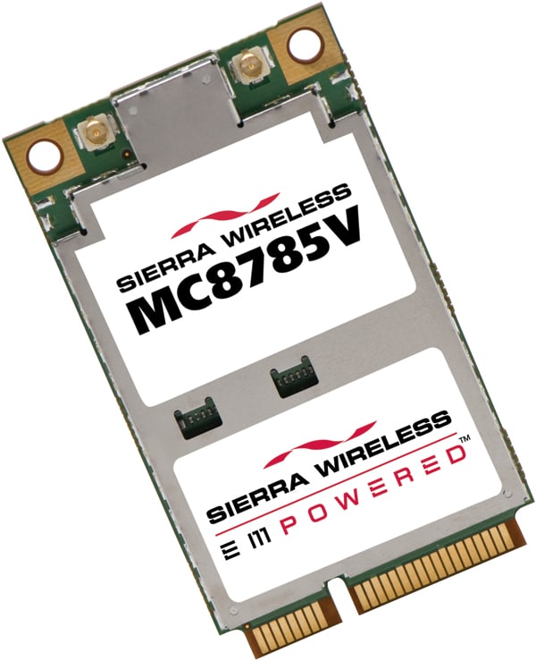
Embedded:
This type of radio is integrated onto the designer’s PCB and enclosed within the chassis. Refer to Figure 2 and 3 for the basic design details. The radio modem has its own shielding and is connected to the antenna connector port via a shielded mini RF cable. The antenna connector is secured to the chassis faceplate to ensure an electrical bond to ground. Overall, this type of radio integration has the best shielding for improved attenuation of interfering signals from within the host device. The antenna, however, when mounted to the antenna port connector now becomes the weakest link due to its close proximity of the chassis near-field emissions. Interfering signals from the chassis can radiate to the antenna and occupy the same frequency bands of operation utilized by the 3G radio modem. Possible mitigation ideas will be explained further in this document.

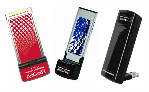
PC-Card, ExpressCard, USB :
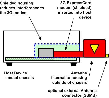
These devices are portable and can be easily swapped in and out of the host device. Refer to Figure 4 and 5 for basic design details. The radio modem circuitry still has its own shielding while the antenna is housed internally within the same enclosure but left unshielded for communications. Once inserted, the modem’s internal antenna is now within close proximity of the chassis and any of it’s near-field interfering emissions. For the PC-Card and ExpressCard, the card slot opening into which they are inserted can also be a way for radiated emissions from within the chassis to leak out and interfere with the card’s internal antenna. To help mitigate this, a good design will include a shielded housing on the PCB, surrounding the 3G card. In some card formats, there may also be an optional miniature RF connector for external antenna installation for improved reception.
3) Antenna
In general, for best wireless service connection of a stationary 3G installation, it is best to be able to have more than one cell site within range for added redundancy and best signal selection. In most cases, this would require an antenna to be more omni-directional rather than a narrowly focused pattern of high gain, locked to only just one cell site. For the embedded modem integration, an external antenna will be required. For the insertable cards, the only antenna available is fixed internally inside the card’s housing. For some card types like the ExpressCard, it can have a miniature RF connector (eg. SSMB) for external antenna connection. Depending on how these antennas are chosen and configured, there may still be problems with interfering emissions from the host chassis. This interference can create issues with the radio receiver’s performance. This performance deficiency has been identified and addressed by the wireless carrier providers as part of the Over-the-Air (OTA) requirements, specifically the test called Total Isotropic Sensitivity (TIS)
OTA Performance
Along with these new opportunities come some technical challenges when integrating 3G radio devices into a host device. As the final step before this product can be operated on any wireless network (eg. Verizon, AT&T, Vodafone, etc.), the product will have to be evaluated to show conformance to their Over-the-air (OTA) performance requirements by a certified test lab such as a CATL (CTIA Authorized Test Lab).
There are two basic requirements:
1) Total Radiated Power (TRP)
2) Total Isotropic Sensitivity (TIS)
These tests are performed in a fully anechoic chamber, representing free space, to determine how well the device will maintain its 3G wireless connection. This article will focus on improving TIS results which are based on radio receiver sensitivity performance.
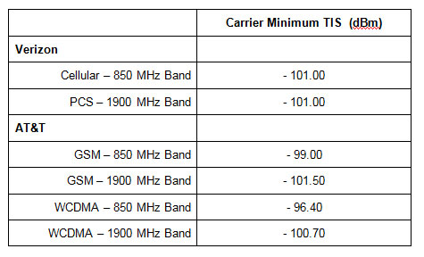
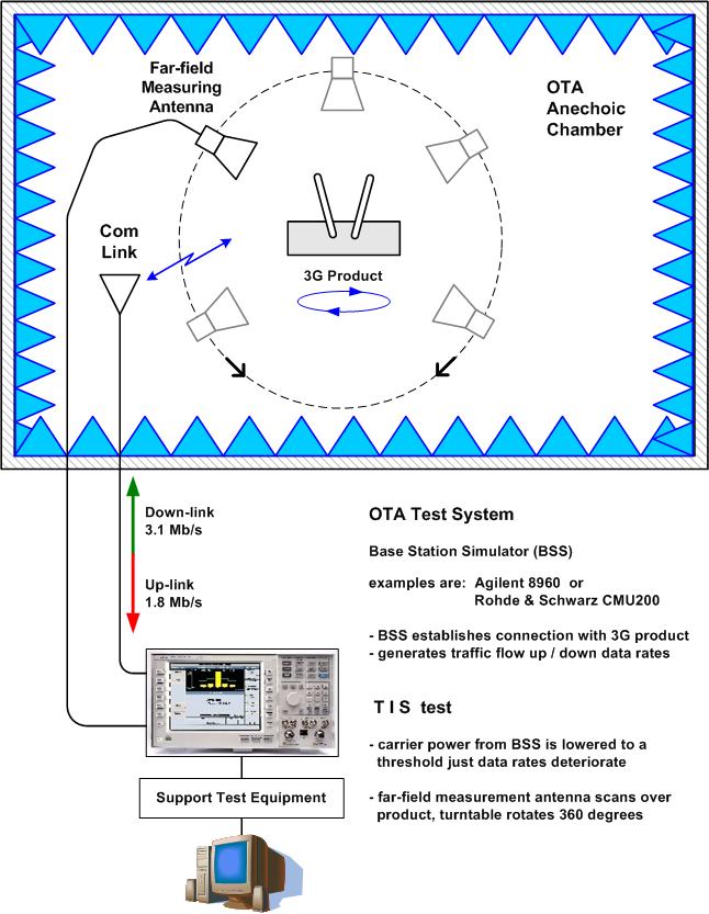
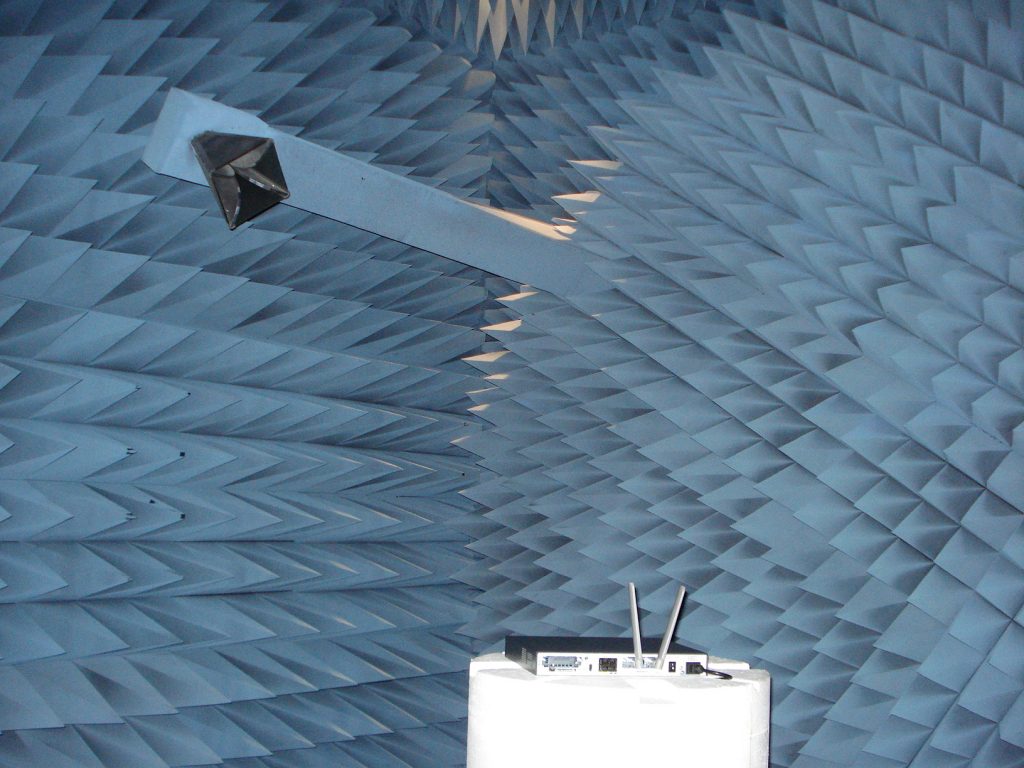
The TIS measurement represents the lowest carrier signal that can be received by the 3G device while maintaining its connection to the cell site and still maintaining download and upload data rates. Tests are performed on many of the mobile channels for each of the frequency bands of operation. Measurements are made with antenna and turntable rotating to create a 3D spherical analysis of the product. Refer to Figures 6 and 7 to view the OTA test setup better. Here are some examples of the minimum TIS levels that the 3G product (as a system) will have to conform with:
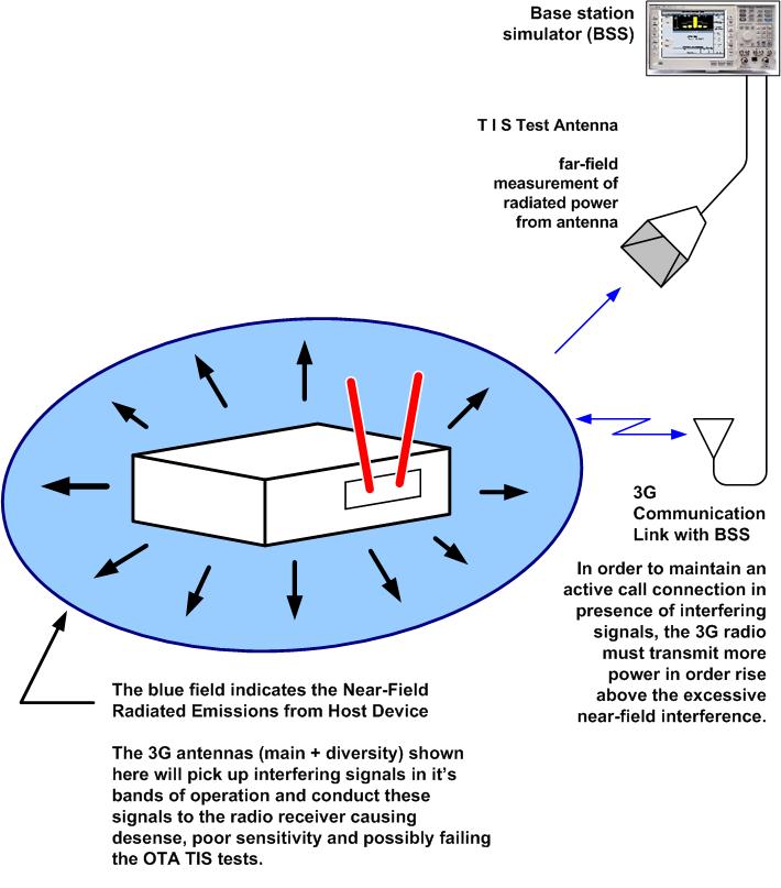
If not designed carefully, some factors can negatively affect the outcome of TIS measurements as shown in Figure 8, 9, 10. Believe it or not, the most common source of interference to the 3G radio can originate from its own host device. This would be its near-field electromagnetic emissions radiating within proximity of the radio and antenna, occupying the same frequency as the mobile channel during a call setup or an active call that’s in progress.
For the embedded modem integration, an external antenna is required. Choosing an omni-directional antenna mounted directly to the chassis’s antenna port connector can be a bad location since the antenna will pick-up near-field interfering emissions radiated from the host device, specifically in the frequency bands of operation. If these interfering signals are strong enough, they will couple to the antenna and swamp the receiver input, causing it to desense. This will cause the receiver to be less sensitive to the incoming communication signal arriving from the cell site and may have trouble either with the initial call setup or during the active call connection.
For the insertable cards, the only antenna is fixed internally to the card’s housing and does not allow for any options. For some card types like the ExpressCard, it can have a small miniature RF connector (eg. SSMB) for external antennas in order to improve signal reception. If an external antenna is used and remains within proximity of the chassis, there can still be potential issues with interference. Typically these express cards have been OTA evaluated and qualified on representative test products. This allows a person to buy these cards directly from the retail store and insert them into their product without any further OTA qualification. In some cases where this insertable 3G card is specifically chosen to be used with a company’s host device, is branded with their own company name and is orderable from them as part of the system, then the wireless carriers may require a requalification to these OTA performance tests at the system level (host device + 3G radio). At this point, the same issues as described above with the embedded radio will potentially have to be addressed by the designer.
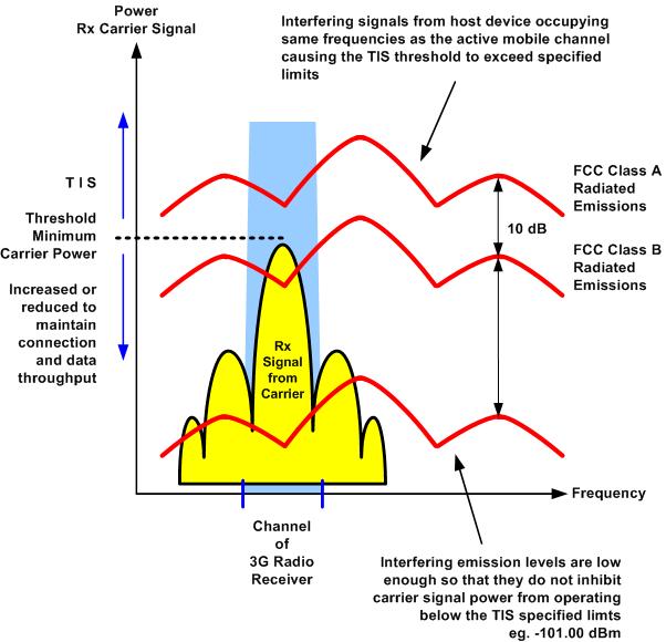
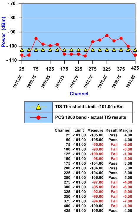
If the system has been evaluated to the TIS requirements and found to be non-compliant, there are a few mitigation options that could be considered. By reviewing the TIS test results (see Figure 10), you can pin point the interfering frequencies which are occupying these operating channels and focus on reducing these emissions. Also note that these TIS measurements are time consuming, have long lead times and are relatively expensive to repeat for every EMC modification, eg. $4000/day. These labs are specialized so they may not be easily accessible to your company, it may require travelling long distances. In other words, it is very important to have a lot of mitigation prep work done ahead time before heading out to the lab. These mitigation steps described below may help with this.
Radio integration into a host device requires a special approach when it comes to PCB track layout and component placement. In order to maintain quality receiver sensitivity performance with passing TIS results, consideration is given to isolating the radio from the chassis’s internal radiated noise emissions. Following this approach will reduce the chances of a PCB respin which is probably the last resort due to its high cost, long delay time to market. Even when the designer has diligently followed integration guidelines, there is no way of knowing or correlating if this product will pass the TIS tests until it actually goes to the CATL lab. Consideration must also be given to the order of testing between the formal OTA evaluation and the EMC tests since they are inter-dependent.
First approach would be to review the chassis construction for any unshielded gaps corresponding to fractional wavelengths of the 3G radio modem operating frequencies and their corresponding channels. Of course any changes made to the chassis will likely have additional retooling expenses.
For the embedded modem integration, pay special attention to the chassis area within proximity of the external antenna. This will typically be the source of the interfering signals leaking out of the chassis, being picked up by the antenna, then down to the receiver.
For the insertable card integration, review the RF grounding effectiveness of the shielded housing surrounding the modem. Also ensure that sufficient grounding contact points are made between the card’s own metal housing and system ground. Review the contact seam between the opening slot in the chassis and the shielded housing.
Perform a proper radiated emissions scan of the product in an EMC chamber, focusing on the channel frequencies that failed the TIS tests. Next, use a near-field EMC probe to locate the source of these interfering signals leaking out from the chassis, making improvements to the chassis shielding as needed. Return to the emissions scan and look for any improvements in reduced emissions. Remember that you cannot use the FCC Class A or B limits as a reference for pass or fail. These interfering frequencies may be much lower in amplitude than the FCC limits but strong enough in the near-field to be picked up by the 3G antenna and causing the radio receiver to desense.
Even if you manage to make notable reductions in the interfering emissions, it will be difficult to correlate these improvements to the actual TIS test data. It is difficult to translate a near-field modification to the far-field measurement in the OTA chamber. Chances are that with these improvements, there will also be improvements obtained but to what degree or how close to passing may not be known until TIS tests are actually performed.
Another debug technique is shown in Figure 11 by using a directional antenna in the near-field and a base station simulator. This method is similar to using the EMC near-field probe, however, instead of measuring the amount of dB reduction in interfering emissions after a modification, the BSS will measure improved up & down peak data rates. This unique test method is based on the fact that if there are interfering frequencies which caused failures in the TIS measurements, this will also cause the data rates to be degraded, similar to when you are in a bad coverage area with your cell phone and the call begins dropping out. A simple modification to the chassis in the right place can improve the upload data rates from 1.2 Mb/s to 2.4Mbb/s. Again, it is very difficult to correlate this to actual TIS measurements, however if you are able to make significant improvements in data rates, you will be much closer to passing the TIS tests.
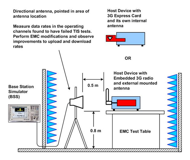
Procedure: Debug Tool – Reducing interfering emissions, improving OTA TIS
1) Establish an active call between BSS and 3G product (over-the-air)
2) Using the BSS, generate optimum up/down traffic flow between BSS and 3G product
3) Lower power from BSS until data rates just begin to deteriorate (monitored on BSS)
4) Observe the peak up / download data rates over one minute, record this rate
5) Perform an EMC modification to chassis or internal circuits as necessary
6) Repeat step 4 and 5 above until delta improvements in data rates are noticed
Note: step 3 is optional, you could just monitor for improved data rates if needed
Notes:
This alternate method is considered to be a debug tool to look for delta improvements in data rates for each EMC modification, much like what an EMC near-field probe would do to help reduce radiated emissions.
There is no guarantee that this host device will conform to the OTA TIS requirements if it meets EMC radiated emissions for FCC Class A or B limits. TIS measurements can fail due to near-field interfering frequencies which may seem negligent in the far-field. With this alternate test method, an improvement in data rate is a good indication that the S/N ratio of the received signal from the BSS has improved. Thus improving chances of meeting the OTA TIS tests. This debug method, however, does not enable you to correlate results into anything meaningful for post OTA TIS measurements.
Antenna and Configuration
Of all the mitigation options noted so far, this may be the only feasible solution which doesn’t involve huge engineering expenses in refabrication of the PCB and/or mechanical modifications to the chassis, incurring long delays to market.
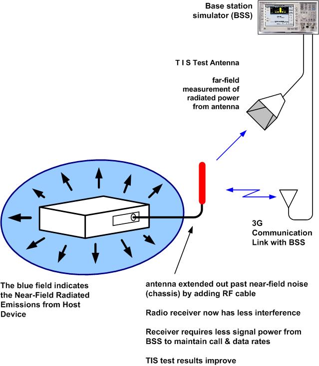
The first recommendation is to move the 3G antenna further away from the noise source, ie. the host chassis. How is this done ? This requires connecting an RF cable in between the antenna and chassis, either as separate piece or integrated with the antenna. An integrated cable will have slightly better performance with insertion loss and VSWR. Refer to Figure 12.
Choosing the right cable type and length is a balancing act when trying to improve the failing margins from the TIS testing. On one hand, the further away the antenna is moved from the noise source (chassis), the lower the interfering signal gets, and better the S/N ratio becomes for the received carrier signal. Unfortunately, any gains achieved from improved S/N ratio is immediately reduced by the cable attenuation, ie. the longer the cable, the more attenuation. If a longer cable is required, the attenuation can be reduced by using a better quality cable instead, eg. changing from an RG178 to an LMR-195 (lower loss).
There will be a magic configuration where the best results can be achieved.
Combination of minimum required distance of 3G antenna from chassis and the maximum cable attenuation allowed will mathematically sum up to an overall dB improvement from the previous TIS results.
Another option may be to select a more directional antenna, called “sector antenna”.
Sector antennas are typically characterized by wide azimuth plane patterns (120 degrees or even wider) with fairly narrow elevation plane patterns. Finding the right commercially available antenna may take some time or it may even require having one developed specifically for the product which would take even longer to do.
Conclusion
Integrating a 3G radio modem into a host device can present some technical challenges in order to comply with the mandatory Over-the-air (OTA) Total Isotropic Sensitivity (TIS) requirements as required by the wireless service providers. One has to consider many factors as described in this guideline: 3G radio form factor, its grounding, antenna selection, careful PCB layout, component placement, improved shielding, and alternate remote antenna placement. When mitigation is required to address TIS failures, there are a couple of measurement and debug techniques one can try, working towards reduced radiated emissions and improved up & download data rates. The business opportunities of an integrated 3G modem for M2M applications is one that can’t be ignored, and hopefully by following this basic integration guide, you will avoid some technical pitfalls and achieve your time-to-market.

