Some applications may require limiting the inrush spike into the input capacitors.
Steve Butler and Jeremy Ferrell, VPT, Inc., Blacksburg, Virginia, USA
BACKGROUND
Inrush current is the spike of current drawn by a power supply when it is turned on. A typical power system is shown in Figure 1. The input EMI filter will include some capacitance connected across the input line. The DC-DC converter will also include capacitance connected across its input and output. The load may include additional capacitance. Each of these capacitors requires current to charge them to their steady state voltage. This current is the inrush current.

Large inrush currents might be governed by a system level specification. There is a concern that high spike currents can create electromagnetic interference in adjacent circuitry, or trip an upstream circuit breaker or the over-current protection of a solid state power controller.
INRUSH CURRENT WAVEFORM
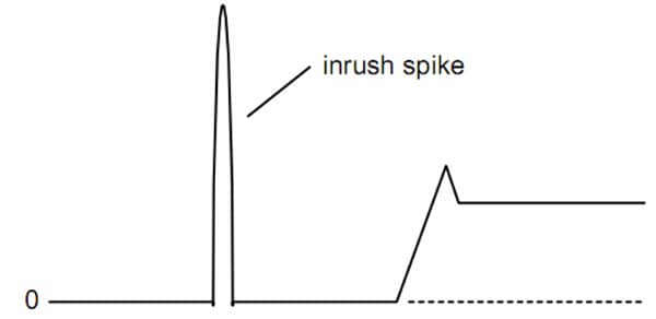
A typical inrush current waveform is shown in Figure 2. It has two current peaks. The first “inrush spike” peak current occurs when the input voltage source is turned on. This peak current flows into the EMI filter capacitors and the input capacitor of the DC-DC converter, charging them to their steady state value. The second current peak occurs when the DC-DC converter turns on. This peak current flows through the power transformer in the DC-DC converter to the output capacitor and into any load capacitance, charging them to their steady state value.

INRUSH SPIKE CURRENT
The first current peak is often referred to as the inrush spike. Its peak value and shape are highly dependent on the characteristics of the input source, specifically the voltage rise time and source impedance. A fast rising input voltage waveform, such as from a mechanical switch closure, will produce a very high and narrow current peak. A slower rising input waveform, such as from the output of some upstream electronics or a capacitor bank, will produce a lower, more controlled peak.
The peak value of the inrush current is determined by the equation, i=C*dv/dt. The capacitance is the total capacitance of the EMI filter and the input capacitance of the DC-DC converter. The dv/dt is the slope of the applied voltage waveform. This inrush spike is only an issue if the input voltage source has a very fast rise time. Normally the only thing that can produce a fast enough rise time is a mechanical switch or relay closure. If the source is a switching power converter, solid state power controller, or capacitor bank, the rise time will usually be much slower. Switching power converters usually have output voltage rise times on the order of a few milliseconds, solid state power controllers (SSPC) usually from 50us to 500us, and large capacitor banks usually cannot be charged in less than several milliseconds. These slow rise times will not produce excessively high current peaks. It is also important to evaluate not only the peak current, but the i2t of the current waveform to determine if an upstream fuse, circuit breaker or SSPC will trip due to inrush current.
TURN ON CURRENT
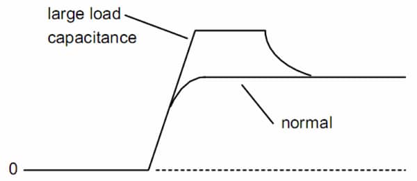
The second current peak of Figure 2 is also considered part of the inrush current. This peak occurs when the DC-DC converter turns on and draws current from the input to charge its output capacitance and any load capacitance. Typical turn-on current waveforms are shown in Figure 3. The turn-on current is the same whether the converter is turned on by applying the input voltage or via the inhibit signal.

VPT’s DC-DC converters utilize a proprietary a magnetic feedback scheme with a well controlled internal start-up sequence and a precise output voltage soft start feature. The voltage soft start feature ensures the output ramps up in a controlled manner, with limited dv/dt. Due to the soft start, the input current usually does not exceed the steady state input current of the converter during turn-on, see the normal curve shown in Figure 3.
VPT’s DC-DC converters also feature continuous constant output current limit. They will supply full rated current into any load, they do not hiccup or shut down and restart. This allows them to start any load capacitor, regardless of size. For cases with very large load capacitance, the DC-DC converter might enter this constant current limit mode during turn-on. In this case the input current would not exceed approximately 1.5 times the steady state input current, see the large load capacitance curve in Figure 3. This is not high enough to cause any interference or trip upstream protection devices. For VPT’s DC-DC converters, this second inrush peak will not cause adverse effects in the system design.
ACTIVE INRUSH LIMITING
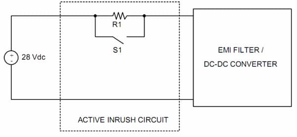
In some applications there is a requirement to limit the inrush spike current into the input capacitors. The only way to do this is to insert a series element into the circuit in front of those capacitors. Figure 4 shows a very basic inrush limiting circuit. The series resistor R1 will limit the input current until the input capacitors are charged. The relay S1 will then close to allow the full current to flow to the downstream DC-DC converter. The relay coil can be driven from the 28V input such that it will be somewhat automatically controlled.

An inductor could also be used to limit inrush current. It would not need to be bypassed since it can carry DC current with low loss. However a large inductance value is usually required to limit the inrush sufficiently. Care must be taken since this inductor can ring with the input filter or can interact with the DC-DC converter’s internal feedback loop, causing system instability. Additional components are usually necessary to damp the resulting resonance.
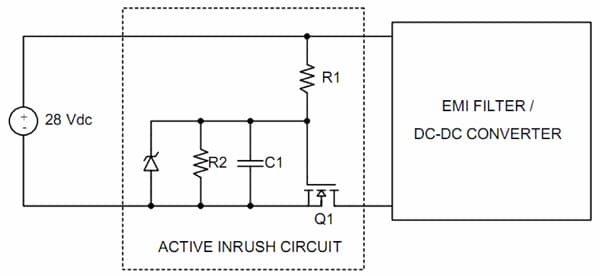
Another practical circuit is shown in Figure 5. This circuit uses a series MOSFET Q1 placed in the negative power lead. Q1 is normally off, with its gate pulled low through R2. When input voltage is applied, the gate will charge through R1. The charge time and turn-on of Q1 will be slowed by C1. R1 and C1 can be chosen to allow the input capacitors to charge slowly, limiting the inrush current. After the input capacitors are charged, the gate of Q1 will charge until it is limited by the zener and Q1 will remain fully on.

This circuit can be modified with Q1 located in the positive lead. It can be driven in the same manner by using a P-channel MOSFET. Or it can use an N-channel MOSFET but with the gate driven by a charge pump or isolated supply. Various other active inrush limiting circuits exist. They all use some series device in the input power leads and act in approximately the same way. It is always important that once the input capacitors are charged, the series device is bypassed or turned fully on to limit line impedance and power dissipation. It is also important that the active inrush control not introduce any noise into the input line since it is located upstream of the EMI filter.
INPUT MODULES WITH INRUSH LIMITING
Several of VPT’s input modules include built-in inrush current limiting. They are listed in Table 1. These modules each use a series N-channel MOSFET in the positive lead. The N-channel MOSFET achieves the lowest ON-state resistance to minimize power losses. Locating it in the positive lead leaves the return path unbroken, simplifying system design. And, this series MOSFET is used for a dual purpose in these modules; it also provides input voltage transient protection.
The DV-704A or DVMN28 contain both an EMI filter and inrush limiting. The two circuits are optimized to work together. The inrush circuit limits any current flowing into the EMI capacitors, but does not introduce any additional EMI into the input lines, as is possible with a discrete circuitry. The VPTPCM-12 contains inrush limiting circuitry which will limit inrush current into its capacitors and those of downstream DC-DC converters. But it also contains switching elements, so it may require additional unprotected EMI filtering at its input.
CONCLUSION
Inrush current is the peak current which flows into the power converter when input voltage is applied or at turn-on. Most system inrush current specifications will be met with VPT’s DC-DC converters alone. Some applications may require limiting the inrush spike into the input capacitors. This will require additional circuitry, or one of VPT’s input modules with built-in inrush limiting.
ABOUT THE AUTHOR
Steve Butler is Vice President of Engineering and Jeremy Ferrell is a Senior Design Engineer at VPT, Inc. in Blacksburg, Virginia. VPT is a vendor of DC-DC converter and EMI filter modules and can be reached ad www.vpt-inc.com.


