Today’s consumers want electronic devices in all shapes and sizes, a demand that can dictate the enclosure design and board shape.
David P. Donaldson, Applications Engineer, W.L. Gore & Associates, Inc., Newark, DE, USA
As electronic devices are getting smaller and as consumers are demanding more features, designing printed circuit boards (PCBs) is becoming increasingly complex—not to mention that any finished design must face both performance testing and testing for compliance with Federal Communications Commission rules and other codes. The typical design process for a new electronic device begins with a marketing team identifying the features needed to respond to market demand, after which an industrial engineer designs the product including key features such as user interface, platform size, enclosure design, and mechanical components. These specifications are then handed over to the component and PCB engineers to lay out all of the circuitry and components.
Many design engineers start by considering shielding requirements, doing such things as identifying the noisy components and placing them as far away from sensitive ones as possible so as to reduce potential interference; however, they also realize that if the product fails in the testing lab, they will have to add cans to the board to provide shielding. To allow space for shielding cans, they may have to group the largest components together to make the best use of these cans. This reactive mindset translates to making the design conform to the shape of the shielding can and designing the board based on shielding requirements rather than seeking an optimal design that maximizes space usage and functionality.

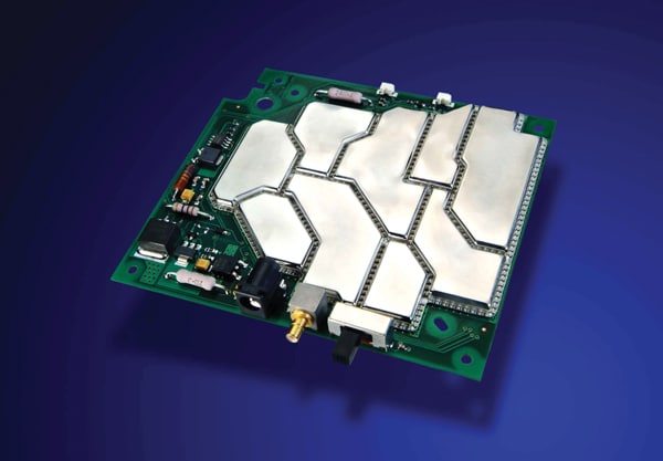
By using thermoformed, board-level shields (Figure 1) instead of traditional shielding technologies, design engineers can place components and circuits on a PCB based on function as opposed to the need to conform to the predefined geometry of the shield. These thermoformed shields allow an engineer to design the board based on circuit and component function without the constraints imposed by the shape of traditional shielding cans. Using a single thermoformed shield provides many specific advantages, all of which result in increased flexibility in board design, integration, and performance.


BOARD DESIGN FLEXIBILITY
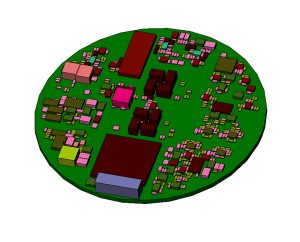
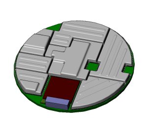
Today’s consumers want electronic devices in all shapes and sizes, a demand that can dictate the enclosure design and the board shape. Stock components and cans are generally square or rectangular, and placing square cans on irregular boards has a significant impact on the engineer’s ability to place components on the board. Thermoformed shields can be shaped to fit any board, regardless of its geometry, without increasing the complexity of manufacturing the shield itself. Designers who opt for thermoformed shields at the outset of a design project can focus on effective board design without being limited by the shape and construction of their EMI shields. For example, Figure 2 shows a round PCB and the corresponding thermoformed, multi-cavity shield that was used to meet code and functional requirements for the device. This board would have required significantly more space for seven separate cans if traditional shielding methodology had been used.
Additionally, thermoformed shields minimize the amount of space needed to shield individual areas. Rather than having multiple cans on a board, each of which needs its own trace to connect to the ground plane, a PCB only needs one thermoformed, multi-cavity shield with a single row of solder spheres to connect the individual cavities to the ground plane. By way of contrast, if an engineer plans to use individual cans to separate two cavities, each can will need its own ground trace with space between them. With a thermoformed, multi-cavity shield, only a single ground trace between the cavities is needed (Figure 3).

The design flexibility of thermoformed shields enables implementation of other necessary features such as mouse holes to avoid coupling, entry points for cables and connectors, and air perforations to facilitate cooling. This flexibility allows components and circuits to be placed in their optimum location without first considering shielding requirements.
INTEGRATION FLEXIBILITY
The design and construction of thermoformed, board-level shields increase available space within the enclosure in a variety of ways. When using stock components and shielding cans, it is necessary to leave sufficient standoff space to eliminate shorting between the tallest component on the board and the inside surface of the can. This additional space can be eliminated by using thermoformed shields because these shields are made of a lightweight, metalized plastic with a nonconductive surface on the inside.
Also, a traditional can has a uniform height, so the tallest component in a shielded area dictates the height of the can for that area. Alternatively, a thermoformed shield allows a design engineer to vary the height of the shield within any one cavity, which in turn provides additional z-axis flexibility to accommodate surrounding components or enclosure features.
PERFORMANCE
Some engineers consider using frame-and-lid technology if they have multiple areas that need to be shielded on a PCB. While this technology provides shielding of each cavity from outside interference, the interior openings between the frame and the lid are susceptible to interference. Thermoformed, multi-cavity shields provide the same level of shielding between cavities as they do with outside interference. In fact, the solder spheres used to install these shields have two millimeter contact points to ensure a high level of product performance of up to 12 gigahertz, and each sphere makes contact with two walls to provide redundancy. On the other hand, frame-and-lid shields guarantee contact by dimples, which are typically targeted at five millimeter spacing. In addition, since the lid is rigid rather than flexible, lid deflection can compromise the electrical contact, and therefore frame-and-lid technology cannot provide the same level of reliable performance.
The material used to construct thermoformed shields is both strong and flexible. The flexible nature prevents the shield from exerting force on the connection points, which enables the shield to maintain reliable contact with the board during both drop and vibration testing.

ONE CASE HISTORY
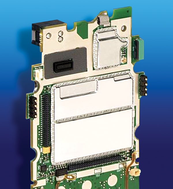
A well-known electronics firm offering automated information and data capture and mobile computing systems was designing a new ruggedized handheld computer with scanning capabilities. The new model needed the potential to integrate up to five different radios in a significantly smaller enclosure than the previous model had. At the very outset before the design process had begun, this company’s designers chose to use thermoformed, board-level shields— a design option that resulted in multiple levels of components on the boards (Figure 4). With this approach, the engineers increased the versatility of their product while reducing the model’s size by seven percent, and the new product successfully passed all testing needed to market the new ruggedized handheld.
CONCLUSION
Effective shielding of all components on a PCB is an absolute necessity if finished products are to pass compliance testing and to function reliably in the hands of the end user. Board designers have often turned to traditional metal can or frame-and-lid technology to provide component shielding. While these options might provide shielding, their metallic construction, size, and rigidity placed constraints on the dimensions and functionality of the finished product. The choice of using lightweight, metalized plastic shields that can easily be thermoformed into any configuration frees the designer to concentrate on creating the optimal design for a reliable product that will fulfil the end user’s expectations.
Dave Donaldson is the global applications engineer for GORE™ SnapSHOT® Shields at W. L. Gore & Associates, Inc., where he has been consulting with customers about EMI shielding options since he graduated from Virginia Polytechnic Institute and State University in 2000. For more information about Gore shielding technologies, contact Dave at ddonalds@wlgore.com.
