Authors
Norm Smith (Teradata Corp.), Jun Fan (UMR), John Andresakis (Oak-Mitsui Technologies), Mark Harvey (Sanmina-SCI), Jim Knighten (Teradata Corp.)
Abstract
Embedding capacitive layers inside the Printed Circuit Board (PCB) have demonstrated the ability to reduce the number of Surface Mount Technology (SMT) chip decoupling capacitors on the PWB surface as well as to greatly improve the performance of the power distribution system. Many systems today utilize this technology, but most public information is limited to data on test vehicles or emulators. This paper involves measurement from actual product and compares the performance of the standard design to one using various types of thin power/ground layers with a reduced number of SMT decoupling capacitors. The radiation from the boards is measured and an investigation into the correlation to power distribution (PDN) noise is performed. A methodology is provided that can be utilized for other designs.
Introduction
The development of embedded capacitor technology has been driven by the need to save board area and/or reduce board size, increase functionality, lower costs and improve electrical performance. Many examples exist for the use of this technology (current capacitive material is used in the high-end computing industry, mostly for telecom and networking applications). For these particular high-end printed wire board (PWB) applications, embedded capacitor technology has been utilized to enhance signal integrity, to reduce impedance at high frequency, and to dampen noise. With clock speeds increasing and tighter regulations on EMI, it is also being investigated to lower emissions from the PWBs and possibly to reduce the need for shielding.
Only a few publications regarding the development of materials for embedded capacitors and the advantages of incorporating embedded capacitors in PWBs are acknowledged here.[1, 2, 3] While some published work demonstrated that the performance of embedded capacitance laminate layers in a PWB stack-up are more effective in high-frequency noise suppression than discrete surface mount technology (SMT) capacitors, little detail is provided regarding the reduction in EMI. This is the primary topic of this paper.
Product Design Review
The standard product is a 12-layer PCB with two 1.5-V planes and one 3.3-V plane, with the stack-up shown in Figure 1. To add the embedded capacitance material while maintaining the mechanical symmetry, a new 14-layer stack-up was used with two thin-laminate cores added. As illustrated in Figure 1, the top thin core is used for the 3.3-V supply, and the bottom one for the 1.5-V supply. The thickness of the 1.5-V/ground plane pair in the center of the stack-up remains approximately the same.
Three versions of the new 14-layer PCBs were manufactured, in addition to the standard 12-layer boards, with three different materials as the thin laminate cores. These boards are denoted as BC24, BC12, and BC12TM in the following descriptions and figures. The standard 12-layer boards are denoted as FR4 for simplicity.
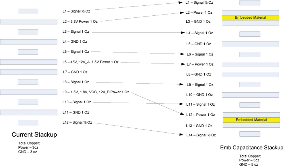
BC24 and BC12 are modified epoxy substrates that are 24 and 12 micrometers in thickness respectively. BC12TM is also a 12-micrometer material but has high Dk ceramic particles added to raise the Dk to 10 from the 4.4 of the unfilled products. The materials are formulated to insure durability during PCB processing. The copper foil is a special low profile version to minimize the chance of shorts or leakage.
To evaluate the performance of the materials, the BC24, BC12, and BC12TM boards were populated only with bulk decoupling capacitors and the FR4 board was fully populated with bulk and high-frequency SMT decoupling capacitors. Compared to the standard FR4 boards, 781 SMT capacitors were not populated in the thin laminates.
Product Performance
Swept-Frequency Measurements of Bare Boards
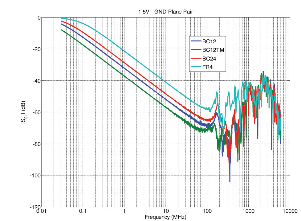
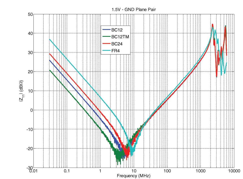
The swept-frequency parameters are good indications of the impedance of the power/ground plane pair. Specifically, Z11 is the impedance of the power bus (power/ground plane pair) looking into a port. It determines the noise voltage generated in the power bus due to a current drawn at the same port. However, Z11 measurements can be dominated by the port inductance at high frequencies. In such cases, transfer impedance, Z21, can reveal information that is otherwise buried in the input impedance results. The scattering parameter, S21, between two different ports in the power bus, which is a function of the transfer impedance, Z21, is often used to study the noise voltage generated in the power bus due to a current drawn from another location away from the observation port. For both Z11 and S21, a lower magnitude indicates a lower noise voltage generated in the power bus due to the same amount of noise current. In other words, the lower the magnitude is, the better the power bus performance.
Bonding pads designed for decoupling capacitors were chosen as the testing ports, and the S-parameters were obtained from a vector network analyzer. Figure 2 and Figure 4 show the |S21| versus frequency curves for the 1.5V/GND and 3.3V/GND pair, respectively, while Figure 3 and Figure 5 show the corresponding |Z21| results that are calculated from the S-parameter measurements.
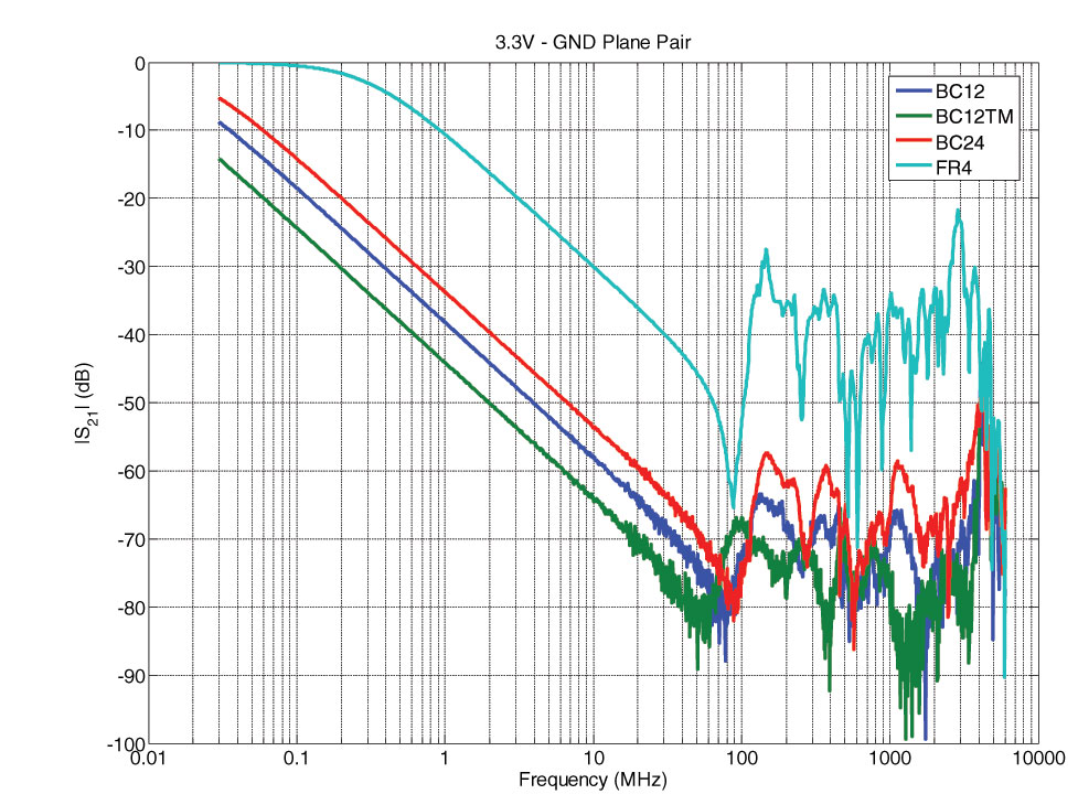
At frequencies below 10 MHz, all the curves clearly demonstrate that the BC12TM boards have the lowest power bus impedance; hence, their performance in noise reduction in this frequency range is the best among all types of the boards. BC12 is slightly trailing behind, followed by BC24. The standard boards are obviously the worst.
When frequency is higher than 10 MHz, as discussed earlier, the |Z11| curves are dominated by the port inductance (notice the magnitude increases at a rate of approximately 20 dB per decade, which indicates an inductive behavior). However, the |S21| curves still show the differences among the boards up to the GHz range. The benefits of the thin cores in these bare boards in terms of power bus impedance reduction are clearly demonstrated, especially for the 3.3V/GND pair due to their lower power bus impedance.
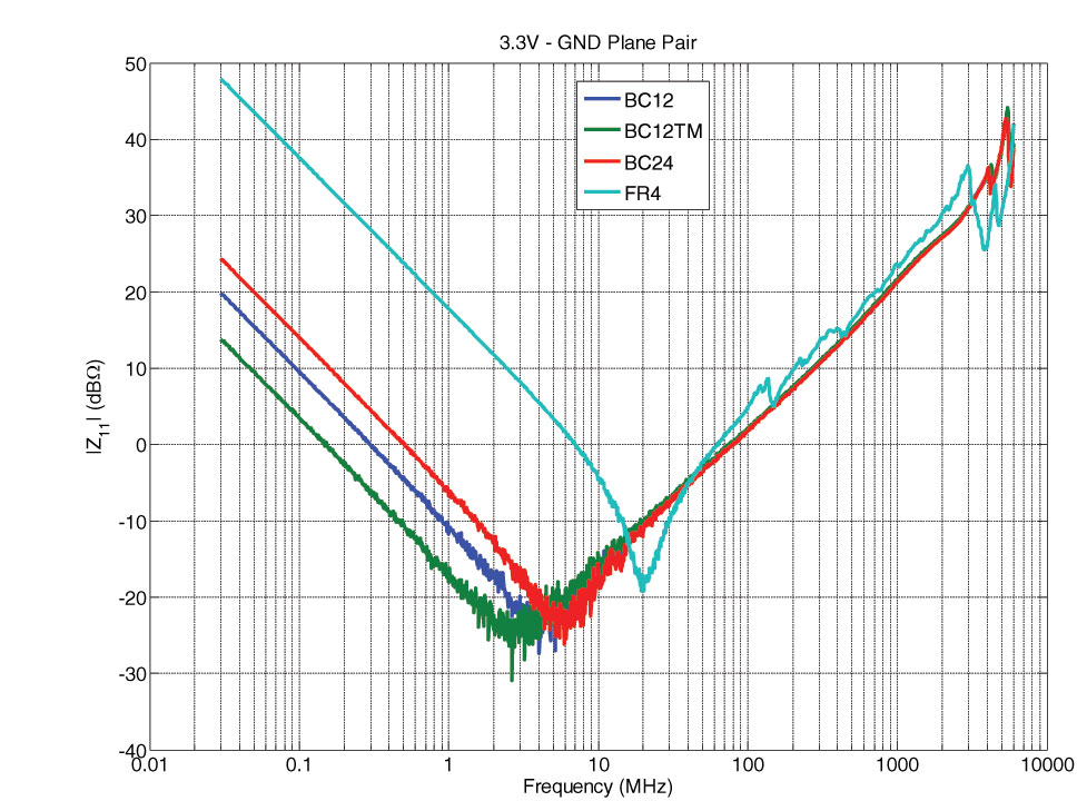
It is worth mentioning that the distributed resonant frequencies in the BC12TM boards are relatively lower than those in the others. This is because BC12TM has a slightly larger dielectric constant, which makes the electrical sizes of the boards bigger.
Two port measurements at the top and bottom of the same via[4] could be used to eliminate the effects of the ports and thus effectively quantify the performance of the thin laminate core. However, in this study, we are not interested in the core itself, we want to evaluate the performance when the core is used in a practical multi-layer PCB. The way we chose to make the measurements resembles what a real IC will see from its power and ground pins.
Time-Domain Power Bus Noise Measurements
Time-domain power bus noise measurements were taken when the boards are running under a pseudo-functioning script. Again, bonding pads for decoupling capacitors were used as ports, and a flexible coaxial cable was used to connect the port to the Agilent Infiniium 54855A Digital Sampling Oscilloscope. The ac noise voltage was measured using a DC blocking capacitor to prevent damage to the oscilloscope.
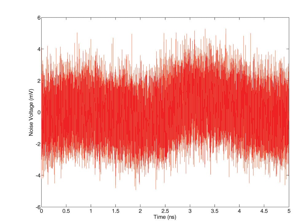
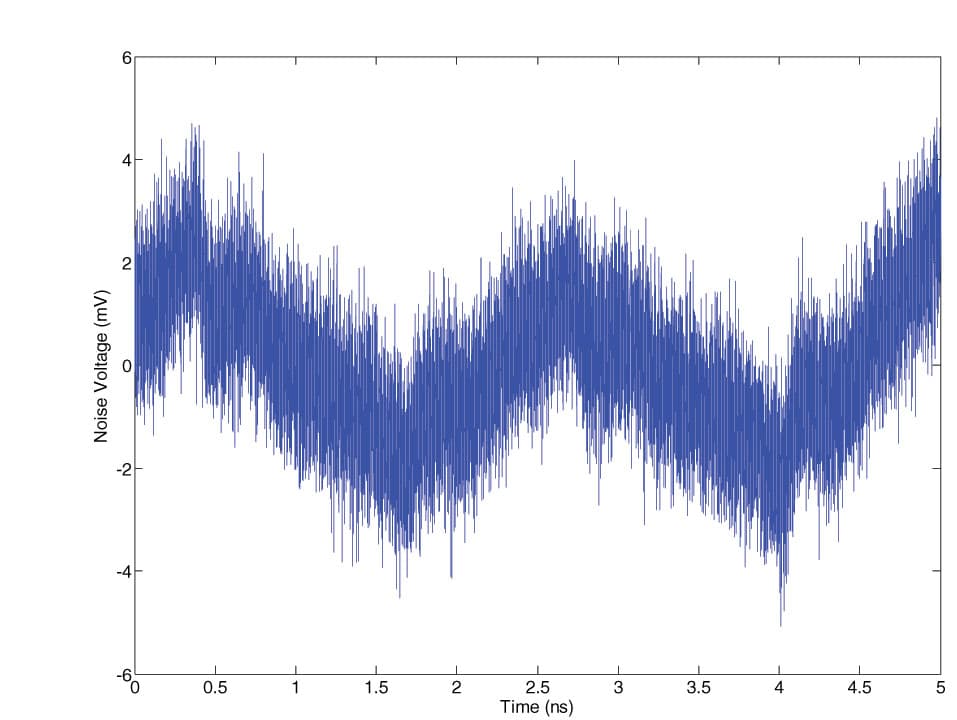
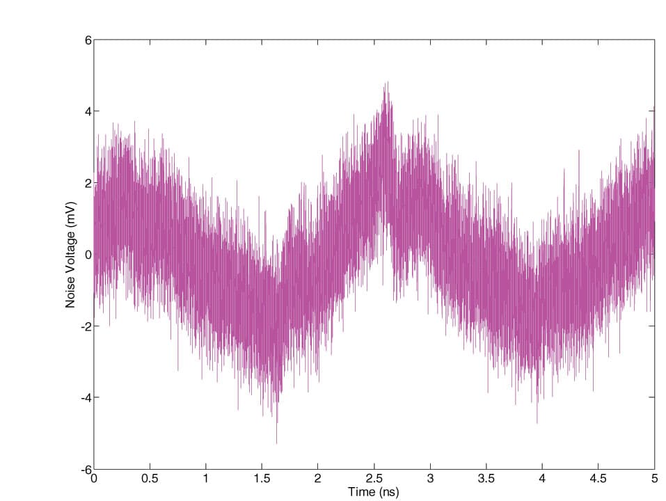
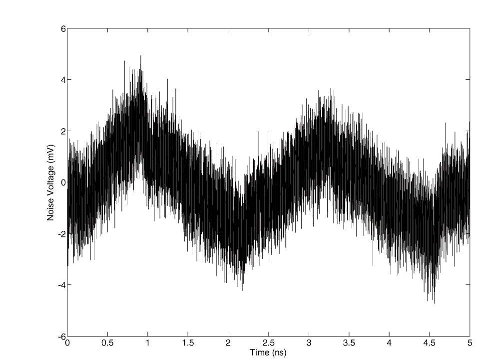
Figure 6, Figure 7, Figure 8, and Figure 9 show the power bus noise voltage in the 1.5-V/Ground pair measured at one location for the FR4, BC24, BC12, and BC12TM boards, respectively. The noise voltages in the 3.3-V/Ground pair at different locations are given in Figure 10, Figure 11, Figure 12, and Figure 13.
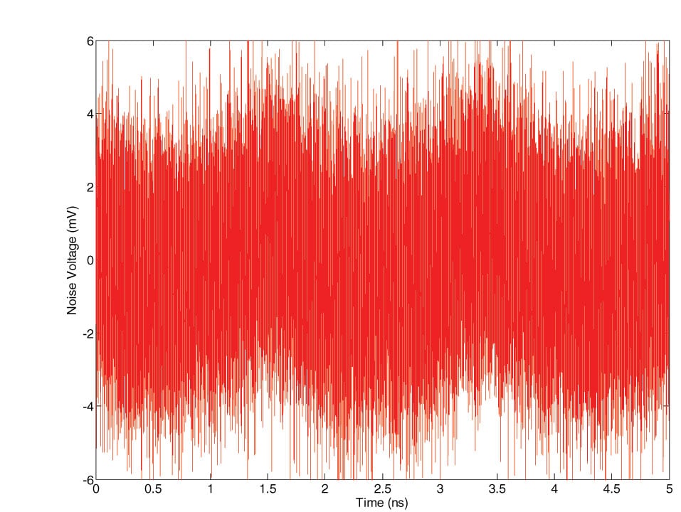
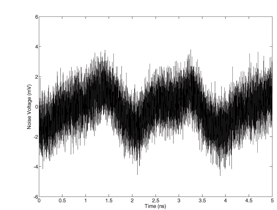
From these figures, the thin laminate boards have comparable time-domain performance, which is less noisy compared to the standard FR4 boards. For the 1.5V/GND pair, the peak-to-peak noise voltages are approximately the same for all types of boards. As illustrated in Figure 6, Figure 7, Figure 8, and Figure 9, this peak-to-peak value is dominated by the lower frequency envelop. The higher frequency noise modulated on the envelope is reduced in the thin laminate boards. For the 3.3V/GND pair, even the overall peak-to-peak noise voltage is lower in the thin laminate boards than the standard FR4 boards,
Overall speaking, the embedded capacitance boards result in lower power bus noise. This is achieved when all the high-frequency SMT decoupling capacitors are removed. It is noteworthy that all the thin laminate boards functioned correctly, with only embedded capacitance layers and bulk decoupling capacitors.
Frequency-Domain Power Bus Noise Measurements
The power bus noise at the same port locations was measured in the frequency domain as well. An Agilent E7404A EMC Analyzer (a spectrum analyzer) was used with a resolution bandwidth of 10 kHz. Again the DC component was filtered away by a built-in DC block.
The results in the 1.5V/GND pair in the frequency band from 10 MHz to 1 GHz are shown in Figure 14, Figure 15, Figure 16, and Figure 17, for the FR4, BC24, BC12 and BC12TM boards, respectively. The corresponding 3.3V/GND pair results are presented in Figures 18 through 21.
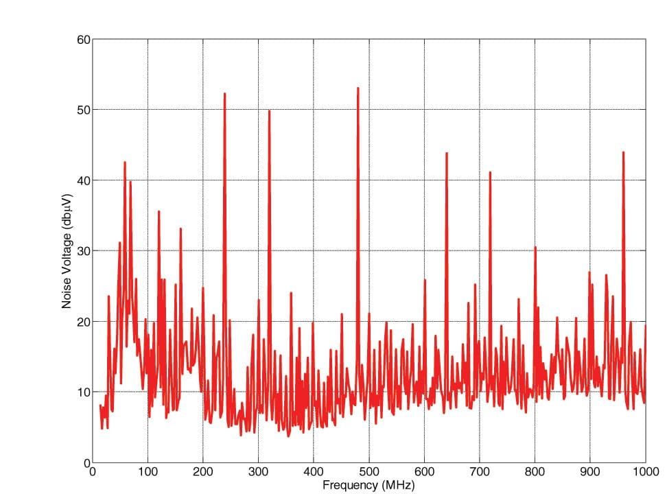
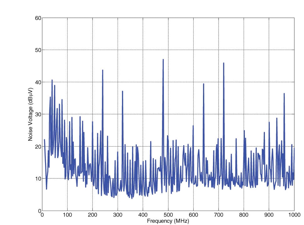
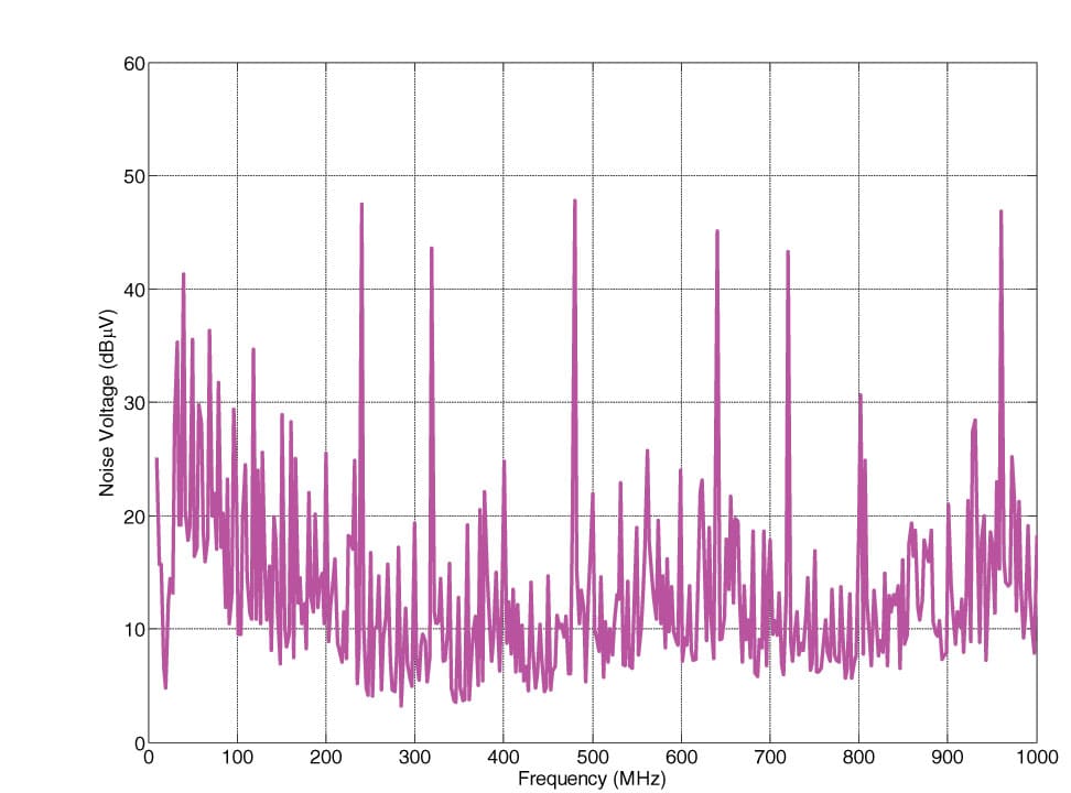
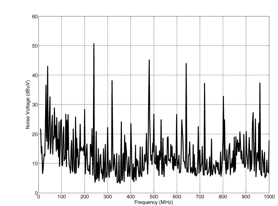
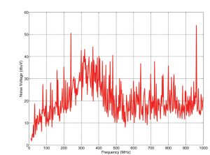
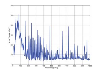
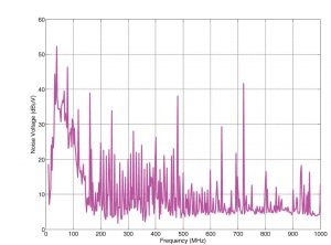

It is quite difficult to draw definite conclusions from these frequency-domain results due to their complexity. Although the noise voltages at some frequencies are lower in the thin laminate boards, for example, at the three peaks between 200 MHz and 500 MHz as shown in Figures 14 through 17, the noise magnitudes at some other frequencies are actually higher. Measurements in the future at frequencies higher than 1 GHz may assist in the development of insight.
EMI Results
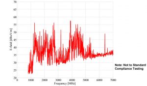
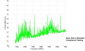
Each of the fully assembled boards was put in the test chamber (in the actual product enclosure) at the Missouri University of Science & Technology and the antenna setup was picked for a 1- to 7-GHz frequency range. This was chosen as the FCC is requiring information on emissions at up to 5 times operating frequency (clock speed of the processor is approximately 1.3 GHz). Measurements were taken with and without the cover of the enclosure in place. It must be noted that the measurements with the cover in place are higher than those that would be measured with compliance testing, since we did not install all the necessary gaskets and shielding.
Figure 22 shows the FR4 control board results. A fairly high peak is present at about 1.8 GHz. With the introduction of the BC24 and BC12 products (Figures 23 and 24) the overall levels of emission are greatly reduced, particularly in the 1- to 3-GHz range. The BC12TM (Figure 25) further reduces the emissions, but also shifts the frequency response. This correlates to a similar shift in the PDN resonances that we previously measured.
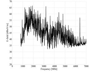
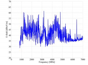

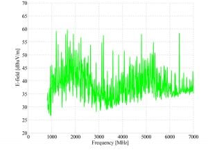
When the cover is put in place, we can see a reduction in the emissions of all the boards (Figures 26 , 27, 28 and 29), but we see a dramatic 10-dB reduction in the maximum peak in the 1- to 2.5-GHz range for the BC24 and BC12 boards. The BC12TM board has even a greater reduction below 5 GHZ, but above 5 GHz the emissions are slightly higher. Figures 30 and 31 show the frequency responses on a single chart for both cases (with and without the cover).

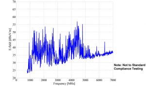
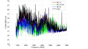

When examining the power bus noise on the PWB with the radiated emissions, it becomes apparent that a reduction in noise has a corresponding affect on EMI. Also, the shift in frequency response due to the different dielectric constant of the BC12TM material is evident in both the power bus noise and the EMI. This needs to be considered if the shift in frequency results in emissions in a critical region.
Conclusions
Several thin laminate materials were applied to a functioning high-speed switch design. The decision to remove all the decoupling capacitors proved to be effective. Initial measurements and simulations clearly demonstrated the benefits of these embedded capacitance materials used as power/ground plane pair, in terms of lowering power bus impedance, reducing power bus noise and the associated EMI (due to this noise). These thin power/ground layers achieved a comparable or even better performance with only the bulk decoupling capacitors.
References
Xu, M.; T. Hubing; J. Chen; T. Van Doren; J. Drewniak; R. DuBroff. “Power-Bus Decoupling with Embedded Capacitance in Printed Circuit Board Design,” IEEE Transactions on Electromagnetic Compatibility, Vol. 45, No.1. February 2003. pp. 22-30.
Ricchuti, V.. “Power-Supply Decoupling on Fully Populated High-Speed Digital PCBs.“ IEEE Transactions on Electromagnetic Compatibility, Vol. 43, No. 4. November 2001. pp. 671-676.
Erdin, I. “Delta-I Noise Suppression Techniques in Printed Circuit Boards, for Clock Frequencies over 50 MHz.” 2003 IEEE Symposium on Electromagnetic Compatibility, Boston, MA. pp. 1132-1134.
Biunno, Nicolas; Novak, Istvan “Frequency Domain Analysis and Electrical Properties Test Method for PCB Dielectric Core Materials.” 2003 DesignCon East. Boston, MA.
Jun Fan received his B.S. and M.S. degrees in Electrical Engineering from Tsinghua University, Beijing, China, in 1994 and 1997, respectively. He received his Ph.D. degree in Electrical Engineering from the University of Missouri-Rolla in 2000. From 2000 to 2007, he worked for NCR Corporation, San Diego, CA, as a Consultant Engineer. In July 2007, he joined the Missouri University of Science and Technology (formerly University of Missouri-Rolla), and is currently an Assistant Professor with the UMR/MS&T EMC Laboratory. His research interests include signal integrity and EMI designs in high-speed digital systems, DC power-bus modeling, intra-system EMI and RF interference, PCB noise reduction, differential signaling, and cable/connector designs. Dr. Fan serves as the Chair of the TC-9 Computational Electromagnetics Committee, the Secretary of the Technical Advisory Committee, and a Distinguished Lecturer of the IEEE EMC Society.
John Andresakis is Vice President of Strategic Technology for Oak-Mitsui Technologies and has over 28 years experience in the manufacturing of Printed Circuit Boards. Before his tenure at Oak-Mitsui, he was Engineering Manager for Hadco Corporation (now part of Sanmina-SCI Corporation) at both their Owego, NY and Hudson, NH facilities. In addition to Hadco, John was in Technical Management at Nelco, Digital Equipment and IBM. He holds a Masters Degree in Chemical Engineering from the University of Connecticut and a Bachelors of Engineering Degree from Cooper Union. He has received eight US (and several foreign) patents related to PCB production and is a member of the IPC Suppliers Technology Council and the various IPC committees developing specifications for Embedded Passives.
Mark Harvey received his bachelor’s degree from Clarkson University in Management and has an MBA. He is a retired Army officer who has worked in the PCB industry for over ten years in both production and engineering. He worked with South Bay Circuits as Processing Manager/Production Manager and later with Hadco (now part of Sanmina-SCI) in Product Engineering, as well as being a UL Compliance Manager. He currently works for Cisco Systems as a Product Lifecycle Program Manager.
Norm Smith is a Design Engineer at Teradata Corporation, San Diego, CA with more than 15 years of service; board level design and high-speed serial links; Bachelors Electrical Engineering Auburn University, Masters Computer Engineering National Technological University
Jim Knighten received his B.S. and M.S. degrees in Electrical Engineering from Louisiana State University in 1965 and 1968, respectively, and his Ph.D. degree in Electrical Engineering from Iowa State University in 1976. He has been an employee of Teradata Corporation in San Diego, CA for 13 years, working in EMI compliance and signal integrity of high-speed digital signal transmission systems. Prior to joining Teradata, he worked for Maxwell Technologies, Inc. and IRT Corporation, where he held management positions and was engaged in the study and mitigation design of the effects of the electromagnetic pulse created by nuclear weapon detonation, EMI, lightning and high-powered microwaves on electronic systems. He has presented numerous technical papers on topics involving various aspects of electromagnetics.
This paper is an update of the paper “Embedded Capacitor Technology—A Real World Example” presented at the 34th International Manufacturing Technology (IEMT) Conference, October 3-5, 2007, San Jose, CA.


