Mart Coenen
EMCMCC
mart.coenen@emcmcc.nl
Arthur van Roermund
Eindhoven University of Technology
a.h.m.v.roermund@tue.nl
Abstract— In 2011, a new concept for resonant-free PDN design has been presented at EMCCompo2011 [1]. This concept is based on terminated transmission lines. From implementations on multi-layer boards some additional constraints have shown up for which solutions are given. On the other hand, the constraints towards a correct application of an on-chip or in-package decoupled device are given based on an actual FPGA device. As this kind of IC-related information is often lacking in the accompanying data sheets and manuals, a compact measurement method to determine the presence and the nature of these on-chip or in-package decoupling is presented and validated by measurements
Introduction
Many of today’s applied IC decoupling schemes are still based on the idea that off-chip decoupling is a necessity to ensure proper operation of the ICs.
However, since more than two decades it is common with CMOS designs to have on-chip decoupling as it would take too long a time of flight to transport the off-chip charge to the on-chip switching event. This on-chip decoupling has then enabled the ICs to reach clock speeds beyond 50 MHz.
Due to this same on-chip capacitance, in combination with the leaded package equivalent series inductance, low-pass filters are formed of which the resonance frequency is well below 100 MHz. Exceptions to these low-frequency resonances are achieved by BGA or leadless flip-chip packages by which transmission lines are formed between the silicon die and the PCB from which supply is taken. However, also in this case their equivalent circuits show steep resonances in the range 100 – 1000 MHz, or even below.
Aside the resonances caused by the on-chip or in-package decoupling with the off-chip decoupling also steep resonances occur on the PCB itself. Most of the PCBs have a isles of decoupling capacitors near to the IC’s supply and ground pins. As these decoupling capacitors form very low impedances at certain frequencies at the various isles on the PCB, standing waves result in-between. The resonant frequencies, n.l/2, are determined by the physical distance between these decoupling isles and the permittivity of the insulating material used with the PCB stack-up.
As presented with the previous paper [1], also standing waves occur from these decoupling areas towards the edges of the PCB which are typically left open. As such resonances occur between each of these decoupled (short-circuited) isles, through the PCB transmission line structure, towards the left-open PCB edges, resulting in m.l/4 resonant frequencies.
Even when two or more transmission lines, with different Z0 and tpd, are placed in parallel with improper termination, new resonances result. The differences in the characteristic impedances: Z0, of the transmission lines will determine the current distribution.
- IC decap characterization
On-chip decoupling capacitances are given by a combination of passive integrated discrete capacitors, typically placed in the package, embedded silicon capacitors (a dedicated die, typically trench capacitors, flip-chip mounted on top) and/or metal-to-metal interconnect capacitance, gate-oxide capacitors or even on-silicon trench capacitors.
On-chip capacitance is typically used with all digital core related CMOS designs: DSP, memory, processor, etc. Also in many cases on-chip decoupling is applied in the digital I/O domain both for the pre-driver, level-shifter as well as for the output stages. W.r.t. analogue circuit designs, on-chip decoupling is less commonly used. However, with the decoupling of oscillators, PLLs, bandgaps, ADC voltage or current references, voltage regulators, etc. more and more on-chip decoupling is needed to avoid any off-chip connection to a PCB reference which has little in common with the on-chip circuit to be buffered or decoupled. Compared to the amount of decoupling capacitance added to the digital domain, only a fraction is added to the analogue domain.
The on-chip decoupling capacitance can be subdivided in two groups:
- Supply voltage dependent
- Supply voltage independent
The supply dependent group is formed by the those which are based on gate oxide capacitance. The main part of this group is formed by all powered standard logic cells which are static in the case where others, to be decoupled, are switching. Their capacitance is determined by the on-chip activity factor: a, where (1-a) of the total amount of cells in decoupling the active ones. Typically, a is less than 0,3 for operating functional blocks.
Other voltage dependent parts are the trench capacitors of which the capacitance is varying with voltage as a depletion capacitance. The process of this decoupling capacitor is borrowed from the regular embedded DRAM trench process. Trench capacitors provide a significant chip-level area saving, using only ⅛ of the silicon area as needed for a standard gate oxide capacitors. Additionally, trench decaps demonstrate dramatic improvements in leakage current reduction compared to standard gate oxide capacitors.
Additional difficulties come in when a complex chip has embedded supply control capabilities i.e. functional blocks on-chip can be turned on or off from the common core supply dependent upon the function the chip has to perform. Aside switching supplies from functional blocks on or off, also supply voltages and/or the clock frequencies at which the functional blocks perform are being varied.
Last but not least, often on-chip supply grid circuitry is no longer accessible due to the use of an on-chip low dropout voltage regulator (LDO). These LDOs are used to control the internal core voltage down to minimize the overall power consumption. However, the integrated on-chip core decoupling must be large enough to overcome a few clock cycles before the LDO can take over, typically between 10 to 100 ns. Additionally, the charge stored in front of the LDO must be capable to provide this instantly for which on-chip decoupling is again inevitable. The time of flight to obtain the charge from an off-chip decoupling capacitor takes too long. A trade-off can be found by the integration of passive capacitors in the package, which can be seen on many commercial devices.
The group of voltage independent capacitances are formed by the metal-to-metal supply grid interconnect capacitances and the lumped capacitors placed in or on top of or underneath the package. In latter cases, the lumped in-package decoupling capacitance is nearby compared to the on-PCB decoupling capacitors but will have some package path length towards the PCB. The combination of these two in parallel with some interconnect length in-between does result in resonances.
III. IC decap measurement set-up
To be able to measure the on-chip capacitance and/or grid impedances, a impedance/gain analyser or vector network analyser is needed. At the impedance measurement port(s) a biasing network is needed to provide the IC to be characterized with its nominal supply voltage at the required supply current. Additionally, all other supply ports, not under investigation, need to be supplied too and, when connected to the same domain as the port being tested, terminated. To enforce the IC under test to be able to power up and to achieve communication via JTAG or some other means to set the supply system into its normal operation state, the IC has to be provided with an external clock. The externally provided clock has to be turned off while doing the impedance measurements at the various supply ports, typically only one at a time.
N.B. During the impedance measurements the IC must be (temporarily) without any internal activity i.e. the externally provided clock has to be switched off.
To perform the impedance measurements correctly, the RF signal amplitude at which the impedance is measured needs to be small compared to the supply voltage applied, this to avoid non-linear behaviour of the IC under test.
To discover the voltage dependency of the decoupling capacitances being measured, the nominal DC bias voltages has to be altered to +5 or +10 % and at least –5 and –10%. When possible, the DC bias voltage shall be reduced down to just above the situation that the device stops ‘functioning’. This non-functionality can be noted by an instant drop of the supply current (even when in hold mode: clock off). This voltage is typically near to the data retention voltage level.
IV. IC decap measurement results
For a state of the art FPGA, the following parameters were found for the digital core:
- On-chip core capacitance: 200 nF +/- 20%
- ESR on-chip capacitance: 1,2 mW
- Chip to PCB inductance: 0,103 nH
- Number of Vcc_core pins: 58
- Capacitance hardly affected by DC bias voltage; 0-0,9 V
The peak current drawn by the digital core (worse case) is slightly over 30 Amps. The average supply current is near to 5 Amps. These parameters, in combination with ideal off-chip decoupling, yield a resonance frequency at 35 MHz with quality factor of nearly 19 !! As can be seen too, a resistive PDN impedance of a few tens of milli-Ohm would enable the reduction of the resonance’s quality factor below 1.
Figure 1 – Simplified FPGA decoupling circuit
In figure 1, the digital core, on the right hand side, is represented by switching capacitors, this to represent the losses of the core correctly. The losses are achieved in combination with the Ron resistances of the switches. The ripple voltage across the core is measured as well as the current through the core, which is mainly drawn from the on-chip capacitance C1. Through the package and the PCB layout off-chip decoupling/ charge buffering is provided by C4 and C5. L5//R5 represent the RF lossy ferrite towards the resonant-free PDN with an RF equivalent impedance of 0,1 W and an ideal supply at DC: L6//R5
Adding this small RF lossy series inductance of 10 nH (L5), in combination with a PDN impedance of 0,1 W, lowers the ground bounce on the chip by a factor of 10 ! Also the on-chip noise would be lowered with a few percent.
To enable power enabling and/or clock enabling large local electrolytic C4 and C5 are added for charge buffering. Note that these electrolytics have to be located at the IC’s supply pins rather than at the PDN side. The amount of RF current through the PDN is proportionally reduced to the ground bounce voltage reduction as switching currents become confined on-chip.
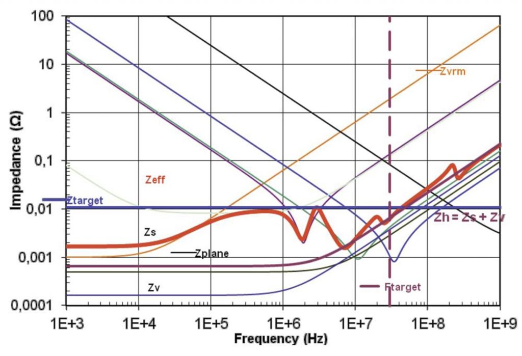
From the fact that the on-chip capacitance is hardly affected by the bias voltage it can be concluded that discrete capacitors are added inside the package, an information which couldn’t be found back in the data sheets. What is made available is a PDN tool which provided the user with the opposite information as derived from figure 1.

Figure 2 – Typical off-chip decoupling impedance to be used with an FPGA, according to the device manufacturer’s provided PDN tool

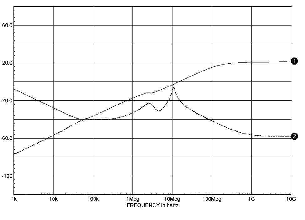
Figure 3 – Impedances as seen by the PDN structure (solid) and as seen by the inside digital core (dashed)
The PDN structure may only be loaded with ‘high’ impedances to maintain the resonant-free PDN condition. The PDN impedance as seen by the core logic needs to be low, at least at the internal clock frequencies used. Be aware that data is either an harmonic or a sub-harmonic of the clock frequencies used.
- PDN resonances
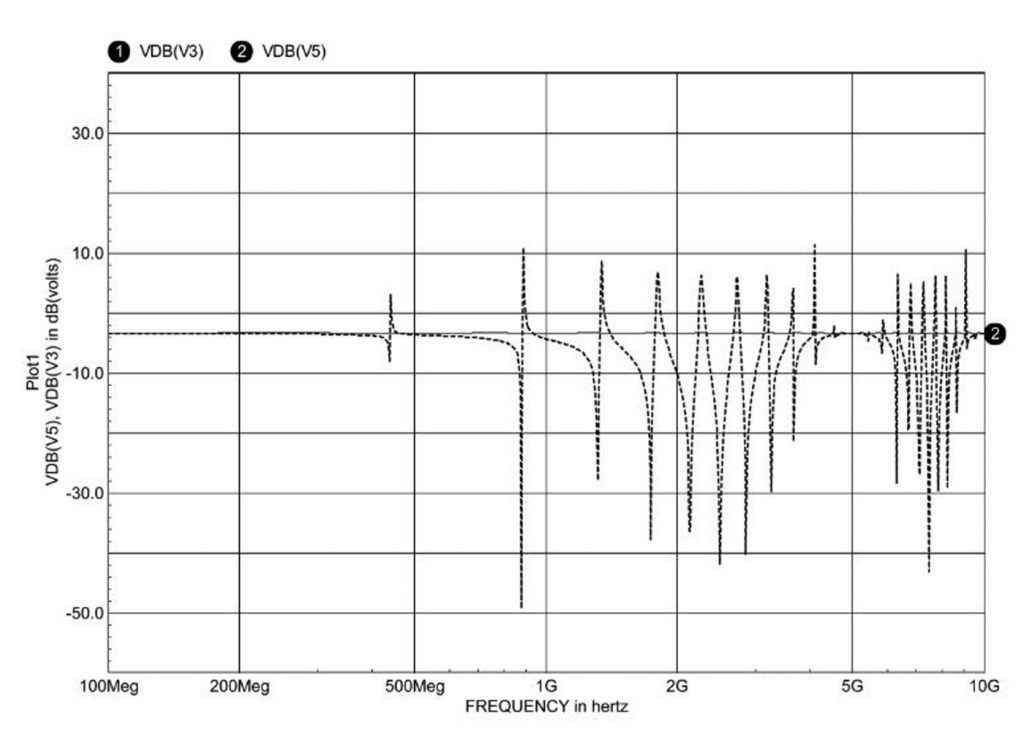
When multiple supply/ground (PDN) planes are used in parallel in a multi-layer PCB stack-up, these can have different materials in-between and also have different spacing in-between these layers, and these should not be stitched together as Z0 as well as tpd will differ and new resonances result, see figure 4.
As can be seen from figure 4, dashed line, only a difference of about 20% in tpd, combined with a difference of a factor 2 in Z0 gives steep resonances on a Eurocard size PCB, already starting to occur below 1 GHz. From this it will be evident that the PCB layer topologies used in parallel with a resonant-free PDN design have to be equally matched to avoid these inter-PDN resonances.
Only when the two or more TL propagation delays are equal, the impedances will behave as parallel placed resistors. When placed in parallel, the edge termination needs to be adjusted to the resulting parallel impedance, see figure 4, solid line and inter-PDN resonances diminish.

Figure 4 – Unmatched TLs in parallel (dashed lines) versus tuned TLs (solid line)
VI. Conclusions
The supply decoupling guidance as provided by the device manufacturers and other PCB experts are debateable and based on an outdated decoupling approach. These outdated approaches are however well-embraced by most of the PCB design community and incorporated into most of the EDA CAD tool environments.
By simple supply decoupling measures, the noise induced on the PDN can be decimated when the on-chip or in-package decoupling measures are known. Even on existing designs an order of magnitude can be improved on ground-bounce and RF emission reduction.
Parallel PDN planes on a multi-layer PCB structure need to be matched, this to avoid inter-PDN resonances. These resonances will occur both with conventional as well as resonant-free PDN design concepts.
When using PDN plane structures with equal propagation delays in parallel, edge termination networks have to be adapted accordingly.
Acknowledgment
The author thanks his customer which whom he had the opportunity to develop this test method. The work carried out is supported by a Dutch Governmental innovation program WBSO, under number: ZT09051042.SO.
References
[1] Mart Coenen, Arthur van Roermund, Resonant-Free PDN Design®, EMCCompo2011
[2] Bogatin, Eric, Signal and power integrity, Simplified, Pearson Education Inc, 2010
[3] Volkan Kursun, Eby G. Friedman, Multi-voltage CMOS circuit design, John Wiley and Sons, 2006 – Technology & Engineering
[4] Renatas Jakushokas, Mikhail Popovich, Andrey V. Mezhiba, Selcuk Kose, Eby G. Friedman, Power Distribution Networks with On-Chip Decoupling Capacitors,Springer, 2010
[5] Special Issue on PCB Level Signal Integrity, Power Integrity, and EMC, IEEE Transactions on Electromagnetic Compatibility, Vol. 52, No. 2, May 2010, Holds over 100 references.
[6] John Andresakis, Embedded Capacitors, Strategic Technology Oak-Mitsui Technologies, 11-2005
[7] 3M, A High Performance Embedded Capacitance PCB Laminate, http://solutions.3m.com/wps/portal/3M/en_US/EmbeddedCapacitance-Material/Home/Learn/WhatIsECM/
[8] Iliya Zamek, SoC-System Jitter Resonance and its Impact on Common Approach to the PDN Impedance, Altera Corporation, San Jose, USA
[9] Om P. Mandhana, Jin Zhao, Comparative Study on Effectiveness of On-Chip, On-Package and PCB Decoupling for Core Noise Reduction by Using Broadband Power Delivery Network Models, Networking and Computer Systems Group Freescale Semiconductor, Austin, Texas, Sigrity Inc, Santa Clara, CA
[10] Istvan Novak, Overview of Some Options to Create Low-Q Controlled-ESR Bypass Capacitors, Sreemala Pannala, Jason. R. Miller, SUN Microsystems, Inc. EPEP2004, October 25-27, 2004, Portland, OR
[11] Minjia Xu, Member, IEEE, Todd H. Hubing, Senior Member, IEEE, Juan Chen, Member, IEEE, Thomas P. Van Doren, Fellow, IEEE, James L. Drewniak, Senior Member, IEEE, and Richard E. DuBroff, Senior Member, IEEE, Power-Bus Decoupling With Embedded Capacitance in Printed Circuit Board Design, IEEE Transactions On Electromagnetic Compatibility, Vol. 45, No. 1, February 2003
[12] Istvan Novak, Comparison of Power Distribution Network Design Methods, Bypass Capacitor Selection Based on Time Domain and Frequency Domain Performances, Comparison of Power Distribution Network Design Methods” at DesignCon 2006, February 6-9, 2006, Santa Clara, CA
[13] Om P. Mandhana, Effect of Resonant Free Power Delivery Network Design on VRM Performance, Networking and Computer Systems Group, Freescale Semiconductor, Austin, Texas
[14] Om P. Mandhana, Modeling, Analysis and Design of Resonant Free Power Distribution Network for Modern Microprocessor Systems, IEEE Transactions On Advanced Packaging, Vol. 27, No. 1, February 2004 107, Jun Fan, James L. Knighten*, Antonio Orlandi**,
[15] Norman W. Smith* and James L. Drewniak, Quantifying Decoupling Capacitor Location, Electromagnetic Compatibility Laboratory, Department of Electrical and Computer Engineering, University of Missouri – Rolla, Rolla, MO 65409, USA
[16] T. Hakoda, T. Takahashi, T. Sakusabe, N. Schibuya., ”Study on Noise Reduction Effect Using the Decoupling Capacitor with Resistor on Power Distribution Line,” Proc. APEMC 2008 (Singapore), pp.878- 881, May 2008.
[17] Scott McMorrow, Teraspeed Consulting Group, Brian Vicich, Samtec, Inc., Steve Weir, Teraspeed Consulting Group, Tom Dagostino, Teraspeed Consulting Group, Pushing the Envelope Without Tears: An Advanced Power Delivery Solution, DesignCon 2008
[18] Junho Lee, Hyungsoo Kim, and Joungho Kim, Terahertz Interconnection & Package Laboratory KAIST, Division of EE and CS Daejon, South Korea, Broadband Suppression of SSN and Radiated Emissions using High-DK Thin Film EBG Power Distribution Network for High-Speed Digital PCB Applications
[19] Iliya Zamek, Nm-System’s Jitter Resonance induced by PDN noise of toggling on-die Logic, DesignCon 2010
[20] M. Coenen, D. de Greef, Optimization techniques for minimizing IR-drop and supply bounce, EMCCompo 2005


