Innovative drop-in SSC solutions effectively manage EMI, preventing costly redesign, reducing production time and maximizing valuable circuit board real estate.
Narendar “Buddy” Venugopal, PulseCore Semiconductor, Campbell, CA, USA
INTRODUCTION
As technology advances become even more sophisticated and applications become increasingly streamlined, traditional methods of EMI reduction are not providing sufficient results for meeting regulatory standards and production requirements. Product engineers who design a full spectrum of high-performance, high-demand consumer electronics applications are turning to innovative alternatives to overcome these obstacles.
REDUCING EMI WITH TRADITIONAL MEASURES
While passive measures of reducing EMI are popular in numerous consumer product applications, they tend to compromise the signal integrity of the clock and other switching signals. Such measures include placing physical resistors, inductors, ferrite beads, and capacitors on the signal path to attenuate any low-pass filter signals. Other methods such as shielding and other mechanical band aids, add cost and weight. On the other hand, spread spectrum clocking (SSC) is an active approach to EMI reduction that attacks EMI at the source—a pulsating clock that generates peaks of electromagnetic energy. This technique involves modulating (increasing and decreasing) the frequency of a clock signal over a period of time thereby “spreading” the electromagnetic energy generated by these switching signals over a selected band of the frequency spectrum, a process that smoothes over the energy spikes of the frequencies and harmonics. This reduces peak emissions to levels that comply with FCC or other regulatory requirements. This technique is particularly effective when applied to the master or source clocks in systems as it provides the spread spectrum benefit to all switching signals derived from these master clocks.
Despite all these advantages over passive solutions, traditional spread spectrum measures do have several drawbacks. For instance, it is highly likely that architectural changes will be needed to accommodate these techniques if they are applied at the source. One example is the need for deep FIFOs or extra pins on an ASIC to ensure that functionality is not compromised. Maintaining clock and data synchronization is a serious challenge that can present itself when these techniques are applied directly to selected independent sub-system clocks. Also, current spread spectrum methods cannot be used in timing-sensitive applications, such as USB.
SPREAD SPECTRUM CLOCKING GOES FURTHER
Limiting or confining the variations in signal frequencies to defined regions corresponding to clock edges can eliminate the potential misalignment of clock and data windows. This design option solves a major drawback of traditional spread spectrum EMI reduction, and there are innovative technologies that effectively reduce the peak amplitudes of clock signals while maintaining synchronization throughout the system and protecting data integrity—thus, eliminating the possibility of cycle slip, which is detailed below. At the same time, Federal Communications Commission (FCC) compliance can be achieved using this type of technology.
ELIMINATING CYCLE SLIP
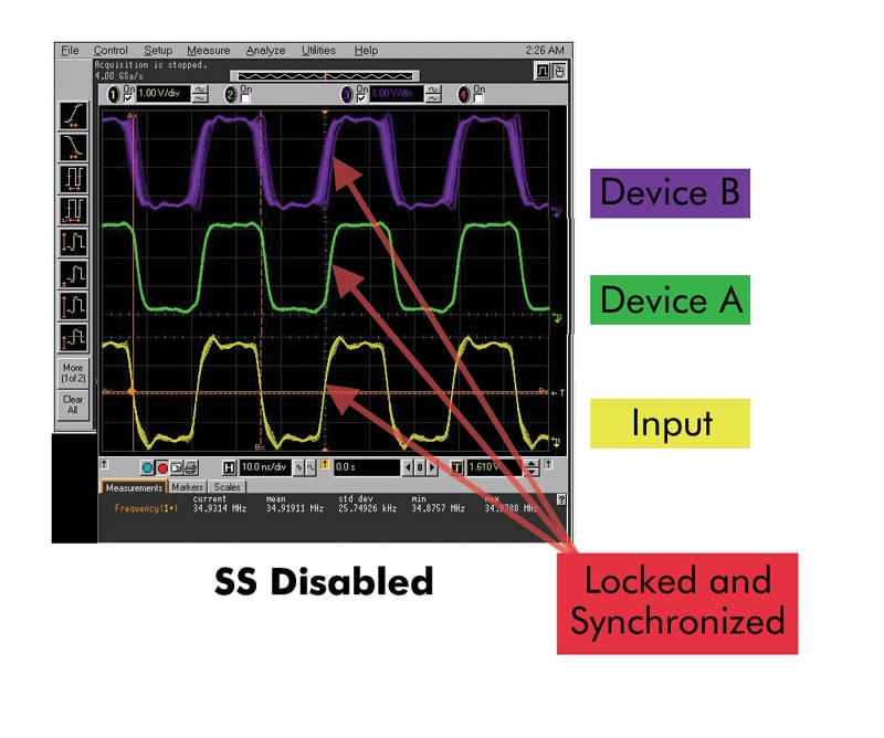
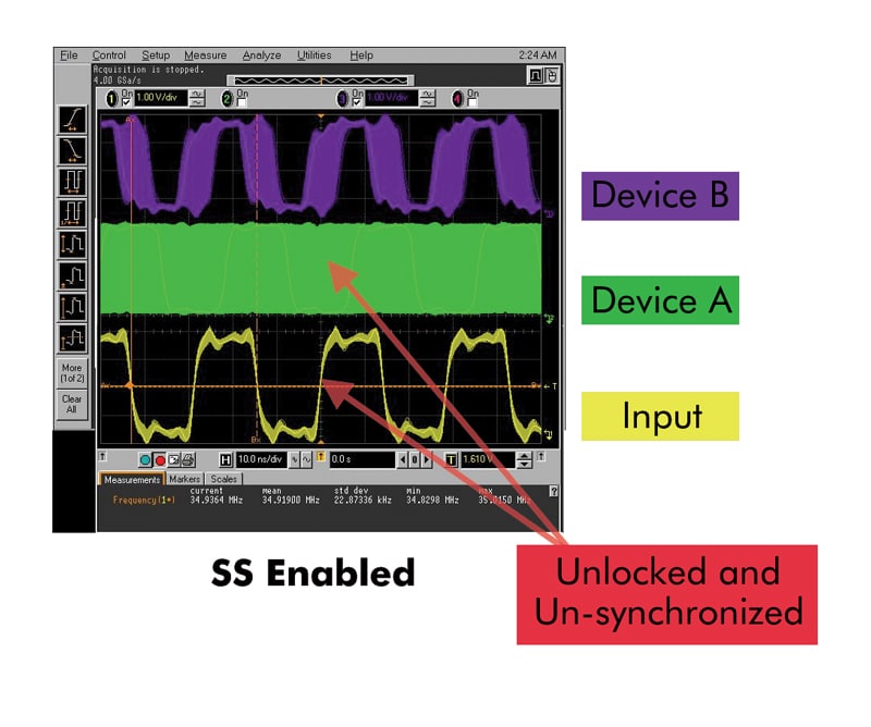
While faster data rates have made FCC compliance a challenge, spreading the master clock at its origin is the first choice in meeting FCC standards and offers an ideal approach. This method keeps the data and the clock synchronized throughout the system. Often, the master clock gets distributed to multiple subsystems. Several subsystems could function well with spread spectrum applied to the master clock. In certain designs, however, subsystem clocks may require independent spreading of EMI. In such cases, the data and the clock can lose synchronization and can produce a cycle slip.
Still, there are ICs that can provide spread spectrum clock modulation for EMI reduction without the associated cycle slip. These devices employ a unique proprietary, patent-pending technology, and they can be inserted directly into the subsystem clock path—providing true drop-in solutions to reduce subsystem EMI on any clock path. These EMI reduction ICs are flexible and can be added at any point in the design process―early or late―to achieve FCC compliance with minimal redesign. See Figures 1 and 2 for a comparison of results from a device that employs conventional spread spectrum clocking and a second device that employs true drop-in spread spectrum technology.


LOWERING PEAK EMI LEVELS IN AN LCD TV APPLICATION
LCD TVs are one example of an application that benefits from drop-in spread spectrum EMI reduction technology. With high-definition video increasingly in demand, LCD TV sales are on the rise. Sales are expected to skyrocket in the United States when all broadcast television stations end analog signals and begin broadcasting only in digital in June 2009. LCD TV manufacturers are preparing to take advantage of this opportunity by offering bigger and better LCD TVs. Unfortunately, an increase in size and performance also produces more EMI. If EMI levels do not meet FCC requirements and a system redesign is required at the end of a product’s design cycle, production time and costs could increase significantly.
When one leading LCD TV manufacturer’s product was nearing the end of its production cycle and did not achieve FCC compliance, the manufacturer needed an expedient solution. Designers needed to address the problem of EMI originating from a 61-MHz low-voltage differential signaling (LVDS) clock. Previously, magnetic-shielding rings had be used to reduce the EMI at the LVDS cable. Increasing the number of rings was considered as a possible solution, but this would have increased production time and costs—and even the size of the cable itself. At that point in the production cycle, this was time, money, and space the manufacturer couldn’t afford to lose.
Applying the new drop-in IC at the LVDS clock dramatically lowered peak EMI levels during subsequent compliance testing. This new technology enabled the manufacturer to meet FCC standards without adding more magnetic-shielding material. The manufacturer was even able to reduce the use of this material by 75 percent, a change that saved valuable printed circuit board real estate and additional production costs.
CONCLUSION
Drop-in spread spectrum technology has dramatically changed the way product engineers can apply spread spectrum modulation techniques to a variety of platforms and applications. By ensuring that timing-sensitive interfaces and IP blocks within systems are not impacted by the altered clock, this flexible and compact technology can now be used easily and effectively in systems that were once ill-suited to SSC because of likely performance degradation and functional failures. This technology is well suited to several applications and interfaces, such as USB, HDMI, and LVDS, among others. Designers can now confidently push the limits of system performance while comfortably meet the growing demands for cutting-edge consumer applications using this true drop-in solution.
ABOUT THE AUTHOR
Narendar “Buddy” Venugopal is a founder, chief technology officer and vice president/general manager of PulseCore Semiconductor. Buddy has 20 years of mixed-signal IC design, operations, marketing and management experience. He holds graduate degrees in electrical engineering and applied physics from the Indian Institute of Science in Bangalore, India; and the University of California, San Diego, as well as undergraduate degrees in physics and electronics.


