Note: The below article has been translated from German and can be found in its original language in the 2011 EMC Europe Guide.
Part 2 of this article can be found here.
Sven König, Langer EMV-Technik GmbH, Bannewitz, Germany
INTRODUCTION
Nowadays, micro-controllers are omnipresent. Whether in MP3 players, mobile phones, washing machines or cars, the small controllers that make our lives easy can be found everywhere.
The properties of the integrated circuits (IC) used in these electronic systems largely determine the EMC characteristics of the entire device. Silicon structures below 100 nm are being developed for micro-controllers. The latest chip sets used in the PC sector have structures of 45 nm and smaller.
This leads to a reduction in operating voltages and operating points which in turn increases the micro-controllers’ susceptibility to interference, in some cases by a factor of ten compared to predecessor models. The logic level, switching time and thus the static noise immunity are reduced. Interference pulses with an edge steepness of less than a nanosecond that enter the IC can thus interfere with its functions.
The increasing circuit integration density in electronic devices also encourages the development and use of ICs in ball grid array (BGA) packages.
In the meantime, micro-controllers are also being offered and used in BGA packages.
The task in hand is thus to examine a current 32 bit micro-controller based on an ARM® Cortex® M3 processor. This works at CPU frequencies of up to 96 MHz and has all the qualities which go to make up current micro-controllers along with a high-speed USB controller. The IC is offered in different types of packages. The controller variants enclosed in a 144 pin low profile quad flat package (LQFP) and in a 144 pin low profile fine pitch BGA (LFBGA) package are particularly interesting in this context.
How do different types of IC packages behave in terms of disturbance immunity (Part 1) and disturbance emissions (Part 2)? Does an IC enclosed in a BGA package have a better immunity than its counterpart in a QFP? Or is its susceptibility possibly higher? Which implications do the in some cases much smaller BGA types have on disturbance emissions compared to a QFP type?
Objective of Testing IC Immunity
The objective is to simulate the test pulses as they occur on ICs during ESD and burst tests of devices. This allows immunity tests on individual ICs independent of the device or module. The IC’s weak spots can be localized by a more precise fault analysis. Specific counter-measures can then be taken in the application. An IC’s EMC characteristics can be taken into account during development by the manufacturer or in applications by the user if they are known. This is the only way to limit substantial economical risks and ultimately ensure a reliable operation.

Test Systems and Conditions
The IC test pulses are defined on the basis of the test procedures for the devices. The respective test set-ups generate electric and magnetic disturbances in the device. These disturbances also have a local effect at the interface to the IC package. IC test generators must ensure a universally applicable and reproducible simulation of these electric and magnetic disturbances. Figure 1 shows the principle on the basis of which burst or ESD is coupled into a device. The test pulse UG(t) that is applied generates a current pulse i(t) that flows through the modules. A voltage drop ∆u(t) occurs in the device. Pulse electric fields E(t) result from the voltage ∆u(t). The current i(t) generates the pulse magnetic field H(t). These fields have an indirect effect on the IC via the conductor runs connected from outside or a direct effect on the IC package.
The magnetic field induces disturbance voltages in the existing conductor loops. A displacement current enters the conductor runs via the electric field. The resulting disturbance current flows into the IC’s internal structures via the connected lines and affects the IC function.
The electric and magnetic fields of very fast events such as an ESD contact discharge are a crucial factor for the direct interference on the IC. The IC’s internal structural design (pin – bonding wire – lid frame – chip) creates loops which are penetrated by magnetic disturbance fields which in turn induce disturbance voltages. Due to the IC’s structural height, internal coupling surfaces are subject to a higher E-field load than circuit board lines, for example. Such E and H fields can also be caused directly by the test generator and result in interference.

The IC test system from the firm of Langer EMV–Technik GmbH has been developed to simulate interference which occurs on an IC during ESD and / or burst tests of devices. The system can be used to test the immunity of ICs under defined conditions and with reproducible results. The probes from the P200/300 series are available for conductive interference. The P200 probes are used to test low-impedance pins such as supply lines whereas the P300 probes are used for high-impedance input and output ports. These generators feature different disturbance characteristics.
Magnetic disturbance fields can be coupled into the IC via the P1200 probe whereas the IC can be subjected to an electric field with the P1300 probe.
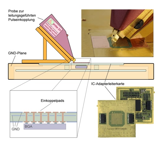
Figure 2 shows the test setup for direct disturbance coupling into the LFBGA package. The IC is fitted to a specially manufactured IC adapter board and the balls are contacted through to the respective coupling pads on the opposite side. The disturbances can be injected directly in the BGA balls via these coupling pads with the probes from the P200/300 series.
The chip works on the basis of its external circuit as specified by the manufacturer. In addition, filter elements are provided in the supply and signal lines to prevent the interference pulse from draining and thus establish defined conditions. The adapter circuit boards including the ICs are inserted in a ground plane and can easily be changed.

Coupling into the TQFP pins is easier since these can be directly accessed with the probe.
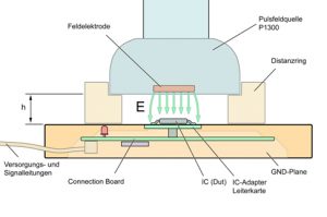
The same setup is also used for pulse field coupling (see Figure 3). This allows a low-cost and quick test of IC immunity to conductive as well as capacitive and/or magnetic interference.
RESULTS
The aforementioned 32-bit micro-controller was tested in a LFBGA package and LQFP package in terms of its immunity to conductive as well as capacitive and/or magnetic interference.
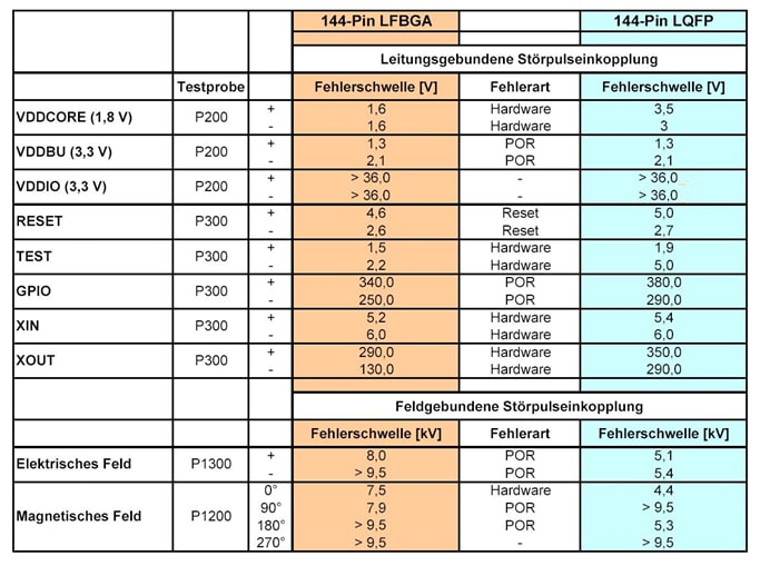
Table 1 lists the results of some susceptible pins and the controller’s susceptibility to electric and magnetic fields in both package forms by way of comparison.

There are only minor differences between the package types for conductive interference pulse coupling into the pins (upper part of Table 1). Both controllers responded to the same disturbance levels with identical fault symptoms. On closer examination, however, it can be seen that the fault thresholds of the controller in the LQFP package are equal to or slightly higher than that of the controller in the BGA package. This may be due to the fact that the impedance of the considerably longer bonding wires in the QFP package dampens conductive interference.
Major differences, however, can be found for different pins of one and the same controller. The core supply (VDDCORE) is very susceptible compared to the supply of the GPIO ports (VDDIO) and its layout has to be considered more critically by the user. The disturbance immunity of the oscillator pins XIN and XOUT also differs greatly.
The faults range from simple data errors, reset triggering right through to hardware faults that cause the controller to stop. Irreversible faults such as a latch-up or defect of the internal oscillator circuit sometimes occur at high disturbance levels. The fact that certain regions of the controller are more susceptible than others is also interesting. The core of the controller with its peripherals is probably located in this region.
Measures that have to be taken by the user to make devices immune to disturbances depend on the design and function of the overall individual device.
Susceptible lines have to be enclosed between GND layers, for example, to block off electric or magnetic fields. In addition, these lines can be protected by filter elements. The blocking capacitors near the supply pin reduce the size of the loop where disturbance voltages may possibly be induced.
There are significant differences when measuring the IC immunity to pulse fields at a distance of 3 mm (lower part of Table 1). The TQFP’s larger surface and thus the larger loops and coupling surfaces inside the package are a disadvantage in this respect. The IC in the LFBGA only displayed interference at high voltages when electric fields were coupled in. The first faults can be detected at 5.1 kV for the TQFP package. The controller in the TQFP package is also more susceptible to ESD magnetic fields. Furthermore, a directional change of the magnetic field becomes clearly noticeable in the test. The first fault occurred with 4.4 kV set in the original direction of 0° whereas the controller remained functional even under the influence of a maximum of 9.5 kV when the probe was rotated by 90°.
These insights in the IC’s behaviour under the influence of pulse fields are decisive for positioning the IC on the circuit board and/or module. E-field susceptible ICs should not be located in areas with a high field strength such as near a metal enclosure. Another possibility would be to shield the IC from external field coupling. Components connected to GND such as electrolytic capacitors near the ICs may already provide protection.
The controller in the TQFP package used in the test would trigger a fault in its original direction under the influence of a pulse magnetic field through a current-carrying metal part. This problem could be solved completely by turning the IC around 90° on the circuit board.
Furthermore, these components should not be located at the edge of the circuit board since experience has shown that this is where the electric or magnetic field strength and thus the interference are at their highest.
SUMMARY
The disturbance immunity results measured on a current micro-controller show that the type of package only has a minor influence on conducted immunity. The micro-controller in the TQFP displayed a higher susceptibility to ESD-H and ESD-E fields. Micro-controllers in BGA packages can thus be used without reservations.
IC manufacturers must have the appropriate know-how to be able to develop ICs with improved immunity. The insights provided by measurements with the test system from Langer EMV-Technik GmbH can be incorporated in IC development. Electronic developers can use these insights in the development of EMC compliant module layouts. The firm of Langer EMV-Technik GmbH offers the appropriate test means to evaluate the EMC characteristics of ICs.
ABOUT THE AUTHOR
Sven Konig is responsible for the test and measurement equipment for electronic semiconductors at Langer EMV-Technik GmbH in Bannewitz. Konig was born in Dresden and studied electrical engineering at the “Studienakademie” in Bautzen. He has been an engineer at the Langer EMV-Technik GmbH since 2007.


