Many electronic components used in highly technological devices can be damaged or degraded by sudden electrostatic discharges, known by the term Electrostatic Discharge (ESD). Components such as transistors, diodes, laser diodes, electro-optical devices, and a variety of integrated circuits are all sensitive to electrostatic discharge. Many manufacturers are increasingly pushing towards miniaturization by optimizing the operating speed: ESD sensitivity of the devices is undoubtedly growing and needs further measures. The damage caused by electrostatic discharges takes place at each stage of manufacture and use of the component, regardless of the electro-optical type.
In the case of laser diodes, a critical problem is represented by current peaks which can interfere with the operation of the device. The laser diodes, for example, have two distinct failure modes with respect to conventional electronic components: one is related to the failure of the junction constituting the base of the device, which is necessarily an electrical overload; and the other is related to the breaking of the optical parts, which is necessarily an energy overload.
ESD features
Damage caused by electrostatic discharge is classified as catastrophic or latent. When it is catastrophic, the electronic device no longer works. When it is latent, the electronic device continues to function even after the discharge, but over time, it deteriorates and breaks prematurely (figure 1).
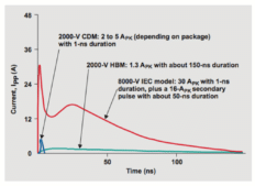
Figure 1: Typical ESD signal [Source: Texas Instruments]
An equivalent generator circuit proposed by the IEC Standard (Figure 2) can represent the typical ESD signal. The circuit consists of the Rc charge resistor (50-100 MΩ), the CS energy storage capacitor (150 pF ± 10%), the Rd discharge resistor that represents the total resistance of the skin (330 Ω ± 10%) and the EUT (Equipment Under Test). The value of the CS energy storage capacitor is representative of the electrostatic capacity of the human body. When the first switch is closed and the second (discharge switch) is open, the capacitor is in the charge phase. Then, the first switch opens, and the discharge switch closes, and then the electrostatic discharge occurs on the EUT shown in Figure 1.

Figure 2: Equivalent circuit to simulate the ESD event
Parts and devices are classified according to their sensitivity to electrostatic discharge following three models:
• the model of the human body (HBM) for the transfer of the electrostatic charge from the human body to a sensitive device;
• the machine model (MM) for the transfer of the electrostatic charge from a charged conductor object, like an instrument or a metallic structure, to a sensitive device;
• the charge device model (CDM) for the transfer of the electrostatic charge from a sensitive object to a conductor, which occurs when static electricity accumulates on the sensitive device through manipulation or contact and then the separation with the packaging materials, the work surfaces or machines.
Some suppressors can be installed on the data lines to reduce the ESD transient. They are connected in parallel with the IC, creating a bridge between the data line and a reference portion of the circuit. There are various options available for ESD protection: SCR diodes, Avalanche TVS diodes and polymer devices.
In the case of an ESD attack, the diode would break and create a low impedance path that limits the voltage and the peak current by diverting the current flow to the ground, thus protecting the IC. Figure 3 compares the peak voltage of a typical ESD without protection with one having circuit protection.
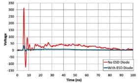
Figure 3: Waveform of a voltage signal with and without ESD protection
A convenient equation for predicting the current I, given a probability P, was derived from the theoretical analysis:
I > 10a pb (RH)c
With A = 4.12 B = −0.645 C = −3.39 within the following range: 0.95 confidence, RH% (Relativity Humidity) comprised between 15 and 55, Probability P(I) = 0.001 < P < 1. For example, the current that will be exceeded only 10% of the time, given a RH% of 20, with 95% confidence is about > 2.2 A.
A calibration setup, simulating the minimum (worst-case) loop impedance of the ESD, is indicated by an RLS series circuit. Its dynamic impedance is approximately 45 Ω, therefore, the ESD voltage signal is equal to measured current peak multiplied 45Ω. For such, in an RLC network with R < 2√(L/C), the discharge is an underdamped oscillatory waveform, with a 20–80% rise time Tr approximately equal to the charging time constant, that is, ≈ 10 ns.
A classic protection scheme like the one in figure 4 takes into account all current paths to avoid thermal (and electrical) damage in the internal circuits, and all voltage scenarios are considered in an attempt to avoid damage to the gate oxides. Clamp1 is the primary protection device for the I/O platform against ESD peaks; Clamp 2 and 3 are isolated from the resistor, and their primary function is to protect the input NMOS buffer. Clamp 4 and 5 protect all internal circuits between any power supply and ground. The diode implementation offers adequate protection for HBM and CDM methods.
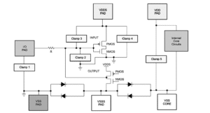
Figure 4: Example of protection layout for ESD [Source: Texas Instruments]
In wireless applications such as GPS, WLAN, Wi-Fi used in many IoT solutions; the antenna can act as a low-impedance path for ESD events to enter the system and damage the circuits. The signal frequencies in these applications can reach 15 GHz, which means that any capacity on the signal paths must be reduced to a minimum to avoid signal degradation. The peak-to-peak voltage of these signals does typically not exceed ± 1 V, so low-capacity ESD diodes can maintain signal integrity and tolerate these voltage fluctuations (Figure 5).

Figure 5: Block diagram of protection for a wireless network [Source: Texas Instruments]
Resistance and materials
The origin of the problem is in the accumulation of electrostatic charges, due to the passage of current through an escape route towards the ground as a restoration of the equilibrium altered by the triboelectric effect (figure 6).
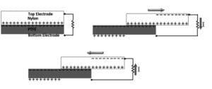
Figure 6: The Triboelectric effect
The triboelectric effect occurs when two different materials come into contact, thus establishing an electrochemical bond between the two surfaces. The charges move from one material to another to balance their electrostatic potential. Some electronic devices, in particular, the complementary metal oxide semiconductor (CMOS) and MOSFET transistors can be accidentally destroyed by these events that cause high voltage electrostatic discharges.
The charge distribution in a material depends on its surface resistivity. In conductive and dissipative materials, the distribution is homogeneous, while it is not homogeneous in the insulators where it is also possible to see charge densification. Very conductive materials with a surface resistance of the order of KΩ have a concise dissipation time, which causes damage if used as a protective device. Other conductive materials with values higher than 10 KΩ behave differently maintaining a reasonable degree of dissipation. The materials that are going to be the best regarding ESD have a surface resistance between 100 Ω and 1000 Ω and go under the name of “static dissipative”. When the surface resistance value exceeds the maximum value, it is in the presence of insulating materials.
Fused silica is an excellent electrical insulator that is used in many optical devices, which maintains high resistivity at high temperatures and excellent high-frequency characteristics. The large band gap inherent in the electronic structure of the silicon-oxygen bond results in electrical conduction limited to the current carried by mobile ionic impurities. Resistivity also has a strong dependence on exponential temperature. Therefore, unlike typical conductors such as metals, resistivity decreases with increasing temperature.
The dielectric constant of the quartz glass has a value of about 4, which is significantly lower than that the other glasses. This value changes little over a wide range of frequencies. The reason for the low dielectric constant is, once again, the lack of highly charged mobile ions, but it also results from the stiffness of the silicon-oxygen network that gives a very low polarisation to the structure.
Laser diodes
Most electronic components rely on a PN junction. Laser diodes are essentially a PIN junction, which differs from the previous one by adding a thin, intrinsic layer. Careful examination revealed voltage fluctuations during the on/off sequences and electrostatic discharge events (ESD) as two significant causes of laser diode failure. The heterojunction is more susceptible to ESD damage than the p-n junction used in conventional components.
A significant increase in overvoltage or overvoltage can cause localized heating and other harmful phenomena that, in extreme conditions, can fracture the laser diode.
During a current change, the emission of laser light can increase to a maximum level, causing damage to the control mirrors, i.e. the optical energy density exceeds the reflective capacity of the integral diode mirrors. When this happens, the optical surface permanently loses its reflectivity, and the laser diode no longer functions properly.
Classic electronic protection devices cannot fully protect laser diodes from electrostatic discharge (ESD) and overvoltage. The goal of these components is essential to block the maximum voltage level across the device terminals up to a preset maximum.
Complicating the design challenges are laser diodes that have an operating voltage that can vary with time and temperature. For example, a 520 nm green laser diode can have a typical operating voltage of 6.4 V and a maximum operating voltage of 8 V. We suppose to choose a conventional ESD protection component with a block voltage of 8.1 V, or more than 25% above the typical operating voltage level. This can constitute a severe danger deriving from the increase of the current of 8 times, considering a dynamic impedance of 1 Ω.
Clearly, the laser diode cannot withstand an increase in the operating current of 8X, even for a short period.
The protection should monitor the instantaneous voltage through the laser diode, including any variations of this voltage and reverse bias. The integrated protection circuit should include a derivative detector, which monitors the variation in voltage across the laser diode pins. If a condition of rapid voltage change is detected, even in the nanosecond range, the device will protect the laser by eliminating voltage variations (figure 7).
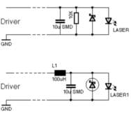
Figure 7: Example of protection for laser diode
Conclusions
The protection of electronic circuits consists of the integration of suitable devices to protect ESD events. The main task is to divert the charge to the ground or in any case far from the sensitive circuit parts. It is very important to define an ESD protection scheme for each device to establish better performance, due to the impact has on product quality.
