How do you decide on the size of a bypass capacitor (or capacitors) for your project? Do you need multiple capacitors to bypass a specific chip? Are multiple value capacitors important for a given use? Do you subscribe to the old Wife’s Tail about having a couple capacitors a couple orders of magnitude different in value in parallel? Here is one take on the subject for you to consider.
Or not…
Is a capacitor just a capacitor?
When you took a class in basic circuit theory in college the professor introduced various types of circuit elements as if they were perfect devices. A resistor only had resistance. An inductor only had inductance. And, a capacitor only had capacitance. “Neglecting fringe effects…” was probably heard by the student from the professor. And, due to the law of primacy (that which you learn first sticks with you) many engineers go on believing this to be true, much to the delight of EMC engineers and technicians as this mistaken belief keeps us gainfully employed.
While the concept of a pure capacitor is a useful tool, in a real circuit there is also resistance and inductance involved. The resistance comes from the fact that our circuit boards aren’t super conductors and the inductance comes from the fact that a circuit has some length and area to it. For this discussion we’ll assume (dangerous word, but…) that the resistance is negligible. Not zero, but close enough for government work. The inductance, however is important.
If we have some small, non-zero, inductance in the circuit we can model the capacitor, as installed, as a series circuit consisting of the capacitor and the small value of inductance.
The value of the impedance of both the capacitor and inductor are dependent on the value of the device and frequency. For the inductor (which we will assume to be 3 nH for this example as that is typical for a bypass capacitor circuit on a PWB) this impedance is
ZL(f) = 2πfL
And for the capacitor this impedance is
ZC(f) = 1/2πfC
As we are looking at a series LC circuit, the total impedance is 2πfL + 1/2πfC
The self-resonant frequency where to total impedance is zero (if we are neglecting the small value of resistance that actually exists in the circuit) is

Below the self-resonant frequency the circuit will appear capacitive and above it the circuit will appear inductive.
Examples
What does this look like as a function of frequency? Let’s take a look at a .1 μF capacitor, in series with 3 nH of inductance, starting at 1 MHz and going through 5 GHz.
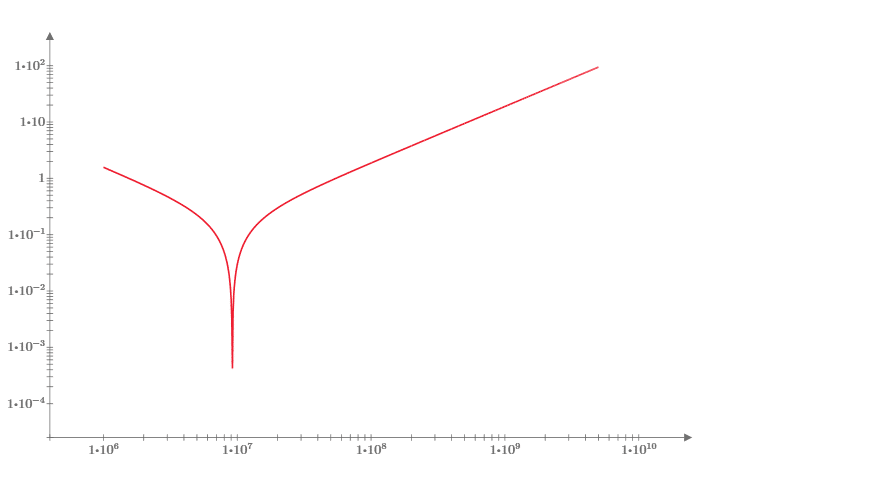
The self-resonant frequency for this LC circuit is just below 10 MHz, so if we were looking for bypassing to be effective for radiated emissions we might think this capacitor is too large as 30 MHz is above the self-resonance frequency for the circuit. Let’s take a look at a smaller capacitor, say 470 pF. What does the impedance of this circuit look like?
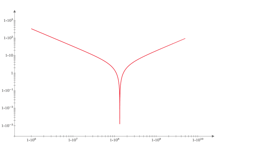
Now we’ve moved the self-resonant frequency up to just above 100 MHz. That looks better. How about making the capacitor an order of magnitude smaller, 47 pF?
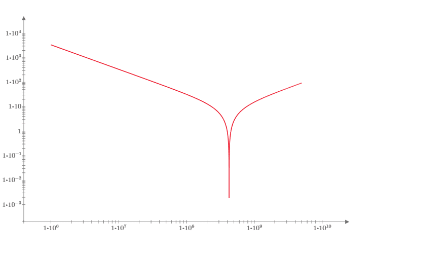
Now the self-resonant frequency is just above 400 MHz. This should be great.
Not quite so fast!
Here’s where the old Wife’s Tale about possibly using a couple capacitors separated by a couple orders of magnitude in value falls apart. Making the capacitors smaller does raise the self-resonant frequency (by the square root of the frequency), but did you notice something else? The overall value of the series LC circuit, perhaps? While the value of the capacitor has changed, the value of the inductance has not. If we superimpose all three curves on a single graph we get
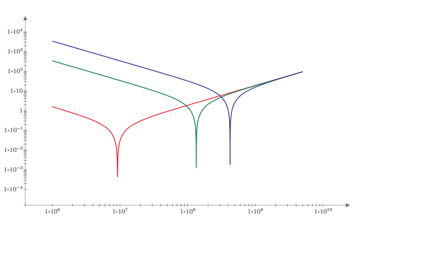
The red line is the overall impedance of a series LC circuit with a .1 μF capacitor and a 3 nH inductor, the green line is the same with a 470 pF capacitor and the blue line is the same with a 47 pF capacitor. Yes, the self-resonant frequency is higher for the smaller capacitors, but the ultimate impedance is the same once we are a bit above the self-resonant frequency. Remember, above self-resonance the overall circuit is inductive, and the inductance hasn’t changed. Also, the impedance of the capacitors goes up as the value goes down for a given frequency. What do we gain by placing a smaller capacitor in parallel with a larger one? Looking at this graph, not much, if anything. What have we lost by adding a second capacitor for each chip? Extra board real estate and decreased reliability, due to the addition of the extra parts.
Now, this example assumes (dangerous word) that adding a second capacitor hasn’t added any inductance to the circuit. Let’s take this a bit further. In the real world that second capacitor isn’t exactly collocated with the first one, so there’s a little bit of extra inductance associated with it. Instead of a circuit that looks like this:
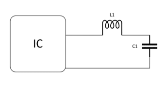
We wind up with a circuit that looks like this:
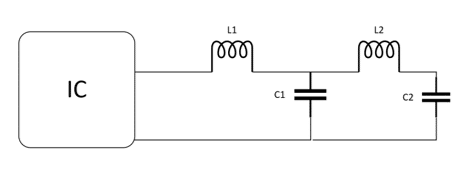
We wind up with a total impedance looking into the bypass circuit of ZL1 + ZC1ǁ(ZL2+ZC2)
If we place the larger capacitor on the side towards the chip being bypassed, we assume that the values of the capacitors are .1 μF and .001 μF and we assume that the additional inductance, L2, is perhaps .5 nH, we get an impedance curve something like this (in green). If we superimpose the new curve on the original curve (in red) for the large capacitor (.1 μf) we see just what the new bypass circuit might look like. Not much of an improvement (if any), is there? BTW, the little blip in the green curve around 200 MHz seems to be an artifact from the math program. Blowing up the resolution to 10 kHz steps and looking carefully at the graph reveals that this blip is gone.
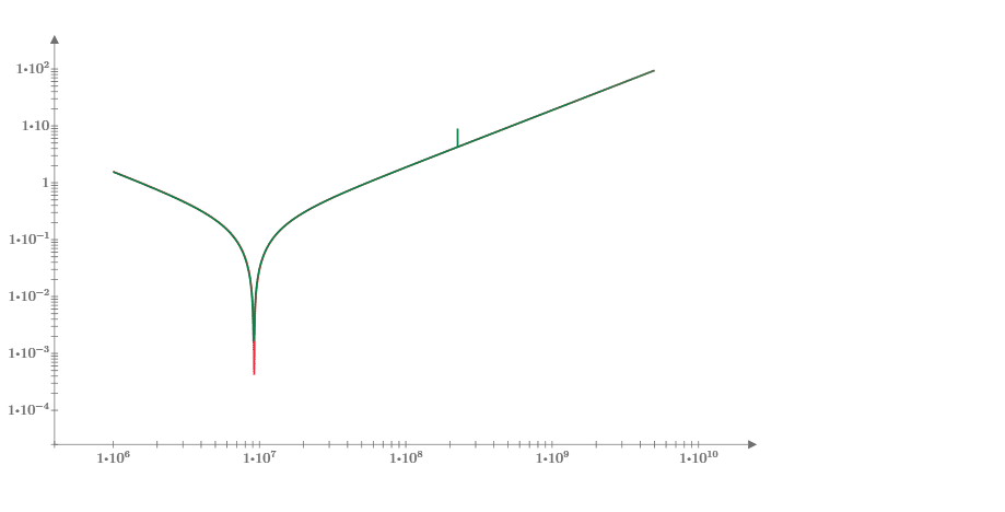
Now, just for fun, let’s reverse the capacitors so the smaller one (.001 μF) is towards the IC and the larger one (.1 μF) is added “outside” the first capacitor. We get a very interesting change to the graph:
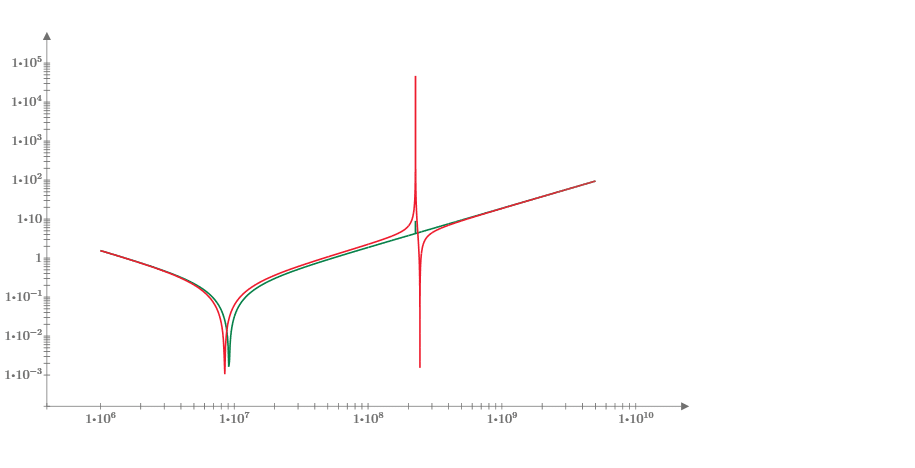
The trace in green is the total impedance of the bypass circuit with the larger capacitor on the side towards the chip being bypassed and the trace in red is the total impedance of the bypass circuit with the smaller capacitor on the side towards the chip. The large “spike” in the overall impedance shows up in this one for the circuit with the smaller capacitor closer to the IC. Also, note that the self-resonant frequency has shifted ever so slightly lower when we reverse the two capacitors. If a harmonic to be suppressed happened to align with the positive going spike (the parallel resonance just below the crossover frequency) there could be serious trouble with emissions.
Given the overall change (and not for the better with the spike in the total impedance) adding a second capacitor that is smaller has virtually no impact if it is placed outboard of the larger capacitor and a potentially negative effect if the smaller capacitor is placed inboard of the larger capacitor. Use a single bypass capacitor.
Now, how big should that one capacitor be?
That’s the 64 million dollar question (and if you are too young to understand the reference, look it up on Google, it’s so old it was a 64 thousand dollar question “back in the day”). There is no one right answer, but keep in mind that a previous employer of the author simply used .1 μF capacitors (or was it .01 μF, I can’t remember) everywhere. And it worked fine. What they did not do was use multiple capacitors of different values for each chip. That capacitor does two jobs. First, it serves as a bypass capacitor to minimize emissions, and second, it serves as a local charge reservoir to allow current to be available to the chip when needed. Those big capacitors where the power comes onto the board are simply too far away to help with this. Their whole purpose is to resupply charge to all the bypass capacitors.
Conclusion
There have been many in the past who have advocated that two capacitors, a couple orders of magnitude apart in value, should be used to bypass chips to minimize emissions. I hope you see why this isn’t a valid idea. The second capacitor doesn’t help, and it costs you space on the board and it costs you decreased reliability due to the extra parts. Not to mention the impact it can have on the overall impedance curve. The only place it helps is your capacitor salesman’s commission.
Have fun keeping the board designers honest, and don’t tell your professors about how their “neglecting fringe effects” statement to sophomore engineering students keeps you employed.


