Earl McCune, RF Communications Consulting
ABSTRACT
Achieving low power supply noise does not automatically assure low EMI. Fortunately a PCB layout designed for low EMI does automatically result in low noise. The techniques presented here do achieve both goals.
INTRODUCTION
Much has been written, spanning several decades, on how to design printed circuit layouts for low EMI [1] [2]. Yet, as a practicing RF engineer I repeatedly encounter boards with layouts that produce significant amounts of EMI. In this age of plentiful information, one would wonder why these problems persist. The answer is not a surprise: much of the information available is misleading and even wrong. A good survey on this is in [2]. Designers therefore choose to learn on their own, which is horribly inefficient and costly. The results presented here have been known for a long time [5]. However it appears that they are forgotten, because they are almost never used. This article is a reminder on how easy low-EMI PC layout really is.
Good EMI design for printed circuits is not that hard, but it does require attention to detail and awareness of the underlying physical processes. And there are no shortcuts. Follow the rules and success is rather easy. Cut any corners and problems rise rapidly.
Electromagnetic theory tells us that there are two conditions necessary to keep EMI at an inherently low level. These conditions are:

1. Minimize the impedance and current encounters
2. Minimize the area of each current loop
By far, EMI publications discuss well how to achieve the first requirement. Essentially nobody though discusses the second criterion. This is the loophole that allows an otherwise low noise board to still produce significant amounts of EMI. Fortunately the solution is straightforward, and easily designed into the PCB layout at the outset. Here we show both what needs to be done, along with why and how well the basic technique works.
First and foremost: know ALL your sources of dynamic currents. The most obvious source of dynamic current is from signals propagating along the signal traces. When these signals have fast edge speeds (2 nanoseconds or less) the board layout needs to have controlled impedance and accurate line source and load terminations. This is the standard fare of signal integrity, and will not be discussed more here. But, particularly when CMOS technology is used, there is another ‘hidden’ source of dynamic currents that, in my experience, is much more of an EMI problem than any signal current.
This additional dynamic current has several names: crowbar current, short-circuit current, supply spike, etc. It is a natural artifact of how CMOS gates are operated inside an integrated circuit, which is shown in Figure 1. In effect, all CMOS gates are composed of switches that alternately connect the gate output directly to the power supply, or to ground, whether the output state should be a ‘1’ or ‘0’ respectively.

The power supply current spike follows from the chip-design criterion that it is not allowed for both switches to be OFF at the same time. Therefore when one is turning OFF and the other one is turning ON, there is a very brief and intentional moment when both switches are partially ON. During this brief instant (usually 1 nanosecond or less) there is a current path (resistance) directly across the power supply, causing current to flow that does not contribute to the output logic signal. This current, though brief, can have a very large magnitude. One small CMOS IC, measured in Figure 2, shows that this spike current magnitude is 300 mA in this instance. Reactances in the current path are excited by the current spike and respond with a damped oscillation. Everything is over in 15 nanoseconds.
Synchronous logic, extremely common in CMOS logic, makes EMI worse because it causes all output transitions to occur close to the same time. This causes all of these current spikes, one for each and every gate in the IC, to happen together. The currents add, of course, making for a very large source of dynamic current. This must be very carefully managed to avoid generating lots of EMI. And this is completely independent from signal integrity.
Electromagnetic radiation is driven by currents, not voltages. The secret to low EMI design is in managing all of the dynamic currents such that the resulting radiation is minimum, though it will never be zero. This effectively quiets any potential transmitter. To achieve this low EMI, electromagnetic theory tells us that the area of each current loop must be made small. How to do this is the trick for low EMI design.
Again, all currents are loops [3]. This we learn in beginning circuit analysis class. Afterwards it is all too easy to forget this fundamental fact when we progress to think that current comes from the power supply, passes through our circuit, and then disappears into ‘ground’. Or worse, to simulate that all current returns are through ‘Node 0’. Both of these common habits obscure reality, which we do at our peril: causing performance degradation, schedule slips from extra work that has to happen, cost increases from EMI modifications and extra testing that shouldn’t be needed, and lost revenue from late product introductions.

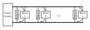
A realistic view of current flow is shown in Figure 3. Signal current loops begin and terminate at the initiating circuit block. Power current loops originate and terminate inside the power supply. Since no practical circuit has zero impedance, Ohm’s Law tells us that there must be voltage drops across all impedances the current encounters around the loop. This includes the return path! As more currents combine in their return to the power supply, the voltage drops across impedances do affect the supply voltage experienced by circuitry such as ‘Block 1’. Hence, it is certainly vital to keep all power and return (this name is much preferable to the word ‘ground’) impedances as small as absolutely practical.
BYPASSING
For high frequency current spikes, which cause all of our EMI problems, it is desirable to give them a return path very close to where they are generated. This is the idea of bypassing, shown in principle in Figure 4. While the total power needed to operate the circuit block must flow from and return to the power supply, the troublesome current spike currents only need to return to the power supply node from where they came.
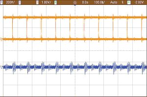
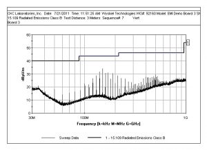
Measured performance of a 2-layer PCB with bypass capacitors at each CMOS IC is shown in Figure 5. This PCB includes copper pour on both top and bottom, with both pours connected to the ground node. Including these pours has a significant beneficial effect [4] and is therefore used here to establish a performance baseline. We note from Figure 5a that the power supply noise is 200 mV peak to peak, and the EMI scan in Figure 5b shows EMI products rolling off above 500 MHz and having a peak around 150 MHz.
When originally conceived over 30 years ago, the addition of bypass capacitors (low AC impedance, high DC impedance) worked very well. This is because the impedance of power and return networks in those days was fairly high. Multi-layer PCB technology was not yet available. Today multi-layer technology is readily available, which is both a blessing and a problem.
POWER PLANES
With multi-layer PCB technology, we are able to dramatically reduce the impedance of both supply and return paths [3]. This is ideal in meeting objective (1) for achieving low EMI. It turns out that this actually makes achieving objective (2) more difficult.
Why this is true we can discern from Figure 4. Each bypass capacitor is connected directly in parallel with the power supply and the circuit block. We again remember from our first circuit analysis class that in any parallel circuit, current will predominantly flow in the path with the lowest impedance. Which path has the lowest impedance? It turns out that when power and return (ground) planes are used, the lowest impedance path is through these planes. So the electrons, being the most lazy (and therefore predictable) creatures in this universe, will flow through the planes. The bypass capacitors have almost no effect, unless the planes are shaped in such a way as they effectively have higher impedance at frequencies of interest.
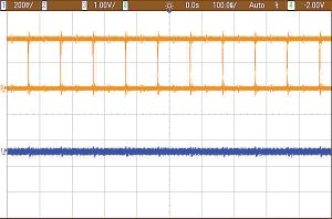
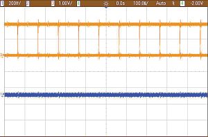
I have seen many circuit boards that behaved the same whether the bypass capacitors were mounted or not. This is the reason why. As a result, we have the unexpected situation where the voltage noise is low, but the EMI is not. Our example board is one of them, as we can see in Figure 6. Taking the same circuit and part placement from the board used in Figure 5, but now using 4 layers with internal power and ground planes, we note a dramatic drop in power supply noise in Figure 6a compared to the measurement in Figure 5a.
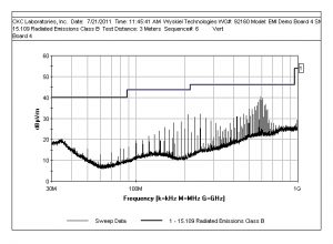
But when we compare the EMI scans, Figure 5b shows a significant increase in the EMI radiation at UHF frequencies. The earlier peak at 150 MHz is gone, but there is now a dramatic increase in radiation above 500 MHz. This is a classic example of how we can reduce noise on the power supply, yet actually make EMI worse. The lower impedance of the power planes is definitely reducing the voltage from the CMOS currents, but the lower impedance is allowing the high frequency currents to flow over much wider area: the high frequency current loops are larger. This is proof that low impedance alone is insufficient to reduce EMI. We need to also force the current loops to be small. One more step is necessary to get what we need.
The trick is to make the power planes look like they have much higher impedance at high frequencies, so that the high frequency spike currents return though the bypass caps and stay completely off of the planes. But at low frequencies we need current to flow through the low impedances that the planes are there for. Fortunately this is readily achieved by inserting an inductive element in the tap to the power plane, as shown in Figure 7.
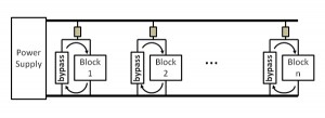
Whenever we have both inductance and capacitance there will be resonance, which is something we do not want. This is addressed by using a very low Q inductor, such as a ferrite bead. This part selection not only dampens out the resonance responses, it also broadens the effective bandwidth of the decoupling—both of which are very good things. The effect of adding this ferrite bead in each CMOS tap into the power plane is seen in Figure 8.

Comparing the supply noise traces of Figures 8a with 6a we see no material difference. Both boards have very low noise on the power distribution. There is a dramatic difference though between the EMI scans in these figures. Adding the ferrite beads has dropped the EMI at 600 MHz by more than 15 dB. Lower frequencies are also attenuated, though not quite as much. But this is the point: UHF EMI products can be inherently reduced in any board using CMOS circuits and power distribution planes, by simply making the bypass capacitors operate again with the insertion of ferrite beads in each tap to the power plane.
This means that both the ferrite bead inductance and the bypass capacitor on the CMOS IC side are vital. They work together in a partnership. Having only the bypass capacitors is worthless when power distribution planes are used. Having only the tap inductance without the bypass caps (I have seen this!) makes things much worse than doing nothing. But together, as we see in Figure 8b, these components are a powerful anti-EMI technique.
Including the ferrite bead into the original PCB design is extremely important. It is nearly impossible to add these later when an EMI problem arises in testing. Admittedly the addition of more components onto a tight PCB is not welcomed, but the price for not doing it is later EMI problems. Compared to the cost of EMI testing and problem mitigation, along with product delays ant those additional costs, the few cents and square millimeters needed for this insurance is cheap indeed.
With large CMOS IC devices, which also have multiple power and ground pins, there is one more step needed to be sure that this technique works. These large ICs usually have power on the chip partitioned into separate regions, meaning that on the chip there is usually not a connection among all of the power supply (VDD) pins and the ‘ground’ return (VSS) pins. It is necessary to identify which VDD and VSS pins go together. The bypass capacitor must be connected between these matched pairs to have the desired effect. It is worthless to ‘bypass’ the VDD of one power region with the VSS of a different region. Though when the bypass capacitors are properly connected across each separate power region of the IC, and then with a ferrite bead in each tap into the power plane, the EMI from the board should look more like Figure 8b than Figure 6b.
CONCLUSION
Low noise design does not guarantee low EMI performance. The converse though is true: a low EMI design for CMOS does result in low supply noise. It is practical to simultaneously get low EMI, even at the microwave frequencies corresponding to high-order clock harmonics, and low noise voltages on power distribution networks in large digital printed circuit boards. The key is to confine signal and transient supply-current loops to physically small areas local to each CMOS integrated circuit. This is achieved with judicious choice of local bypass capacitors and adding inductive elements between the power distribution network and the IC / bypass capacitor parallel combination. It is important to assure that the bypass is connected between associated power (VDD) and ground return (VSS) pins for the particular IC.
These low EMI design techniques are very difficult to impossible to insert into an existing PC board that does not already use them. This simultaneous minimization is therefore something that must be designed in at the beginning. Doing so eliminates many of the problems encountered during EMI certification testing of the product before sale.
ACKNOWLEDGEMENT
The author is extremely grateful to CKC Laboratories, Inc. (www.ckc.com ) for their generous support of the formal EMI measurements at their Fremont, CA facility.
REFERENCES
[1] B. Archambeault, “Eliminating the MYTHS about printed circuit board power/ground plane decoupling, ITEM 2001
[2] L. Ritchie, “EMI: What It is, Where It Comes From and How to Control It,” The PCB Design Magazine, April 2013, pp. 10-18
[3] E. McCune, “Ground Current Control Enhances Dynamic Range in High Speed Circuits,” EDN Magazine, January 19, 1995 (available at http://www.edn.com/article/493741-EDN_Access_01_19_95_ Ground_current_control_ enhances_dynamic_range_in_high_speed_circuits.php)
[4] E. McCune, D. Wyskiel, “Low-EMI Printed Circuit Board Design for High Frequency Waveforms,” RF Technology International, August 2012, pp. 10-21 (available at http://rfti.com/wpcontent/uploads/2012/09/RFTI0812_McCune-Wyskiel.pdf )
[5] M.J. Coenen, “ElectroMagnetic Compatibility (EMC) and Printed Circuit Board (PCB) constraints,” ESG 89001, Philips Components, 1989. http://alt.ife.tugraz.at/datashts/Philips/8096.pdf
AUTHOR BIO
Earl McCune has more than 40 years of experience in radio and wireless technology, including circuit- and system-level designs. He is a graduate of UC Berkeley, Stanford, and UC Davis. He is also a serial entrepreneur in Silicon Valley, cofounding Digital RF Solutions (1986-1991) and Tropian (1996-2006). He regularly presents at international conferences and workshops, and is an instructor with Besser Associates. As an inventor and co-inventor he has 64 issued US patents. Contact him at emc2@wirelessandhighspeed.com.


