Introduction
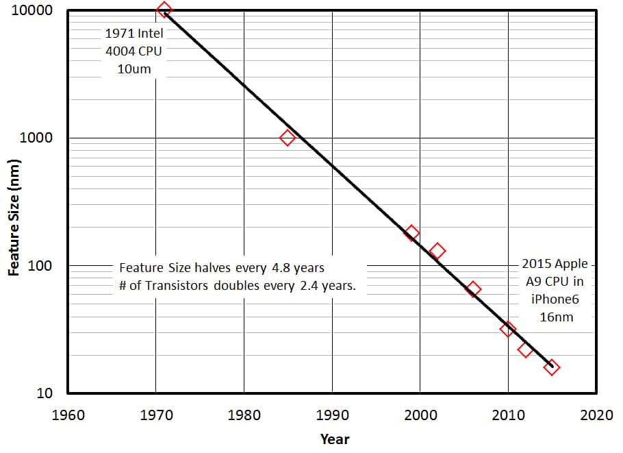
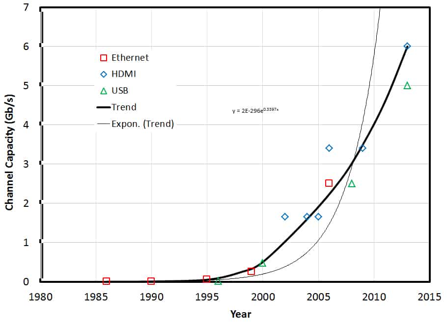
Correctly choosing an external (off chip) Transient Voltage Suppressor (TVS) is not as simple as it once was. Integrated Circuit (IC) feature size is shrinking (Figure 1) and more and more inputs are being exposed to the outside world. Portable consumer devices are everywhere and have more functions in smaller and smaller sizes, necessitating smaller and smaller TVS packaging. At the same time, the demand for bandwidth is sky-rocketing, as witnessed by three popular technologies: Ethernet, HDMI and USB (Figure 2).
System Level Considerations
Failure Levels of Unprotected Inputs
The first constraint to be considered is the failure level of the input to be protected. Hopefully, this will be known based on Transmission Line Pulse (TLP) or Human Body Model (HBM) testing, but this is often not the case. If it is not known, and cannot be measured, a reasonable estimate must be made.
Symbol Rate
The symbol rate of the application must be known. This is not always the same as the bit rate. For complex modulation schemes, the number of bits per symbol can be much larger than one. In some simple modulation schemes the number of bits per symbol can be less than one. Typically, the analog bandwidth required for a digital signal is between half the symbol rate and the symbol rate. For example, if a digital protocol requires a symbol rate of 5Gsymbols/s, then the analog bandwidth required is between 2.5GHz and 5GHz depending on channel noise and other factors.
System Protection Level Requirements
The requirements for system level protection must be known and understood. There is a huge difference between a person shuffling across a carpet with a smart phone and a 10G Ethernet Inter-Building Cable subjected to a near lightning strike. There are standards available for all likely Electrostatic Discharge (ESD) and surge threats; these should be used along with applicable protection device datasheets to determine a good protection scheme.
Protection Device Considerations
Insertion Loss
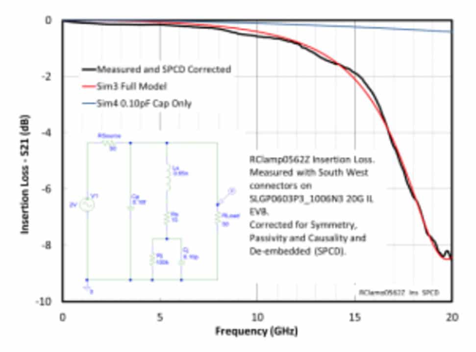
Any device added to a communication channel will introduce extra signal losses in that channel. These losses are caused by the parasitics of the added device. Often, only the capacitance is considered, but especially for low capacitance devices, the stray inductance has a very large effect. Figure 3 shows a comparison between a measured part, a full model simula tion for the part, and a simulation using only the part’s junction capacitance. It is quite apparent that there is a large difference even well below the -1dB point.
Using Silicon TVS Diodes
Silicon TVS diodes have been used for many years as protection devices. They consist of one or more TVS diodes and possibly one or more steering diodes. Capacitance can cover two orders of magnitude or more; there really is no typical, nor a typical reduction magnitude. The steering diodes are used to reduce capacitance and, in a bridge configuration, allow a uni-directional TVS to symmetrically clamp in a bi-directional fashion.
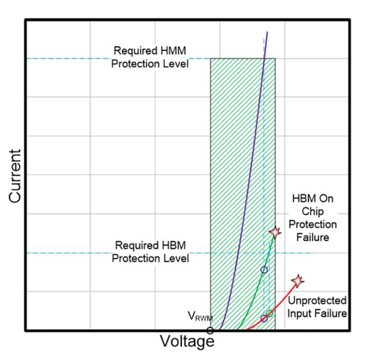
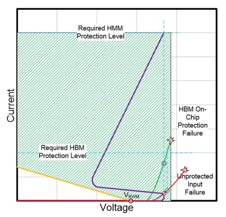
The TLP characteristic of the TVS protection device must include very low leakage at the maximum port voltage (VRWM) and the clamping voltage at the Required Human Metal Model (HMM) protection level must be lower than the Human Body Model (HBM) on-chip protection Failure Voltage, as shown in Figure 4. With increasing frequencies and decreasing on-chip protection levels, it has become more difficult to satisfy both of these criteria while still meeting insertion loss, size and cost requirements.
Using Snap-Back Devices
Snap-back devices can either be of the shallow snap-back or deep snap-back types. An example of a Shallow Snap-Back device would be a Bipolar Transistor (BJT) especially designed for enhanced collector-emitter punch-through breakdown. These devices exhibit low capacitance for their protection levels and are very good for protection in the 1.5V to 4V working range. Deep snap-back devices are typically a 4-layer PNPN SCR type structure. A much larger “window” is available for the external protection device Figure 5.
Avoiding Latch-Up
The major concern for snap-back protection is the avoidance of latch-up. Latch-up can occur if the protection device enters its snap-back region and sufficient DC current is sourced into the protected line to hold it there. Most typically, this occurs due to pull up resistors on the signal line.
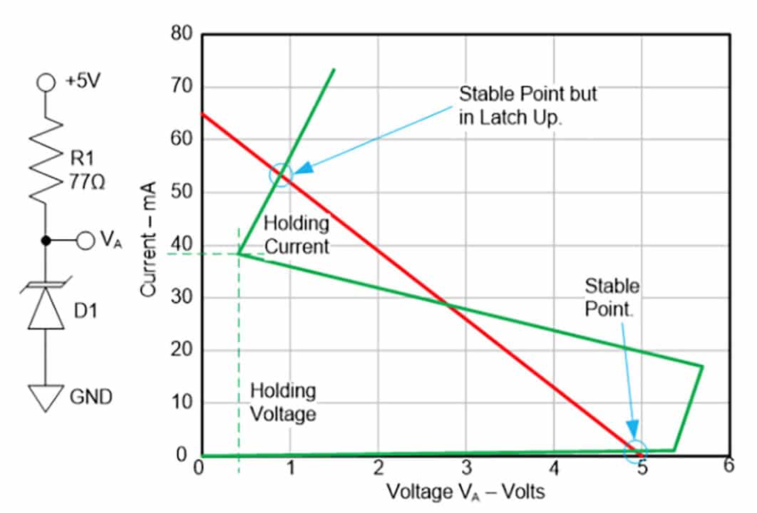
Figure 6 shows an illustration of the problem. The red line is the locus of the operating points of the resistor R1, note that the X-axis is VA – the voltage at the node where the resistor and protection device connect. The green line is the locus of the operating points of the protection device. There are three points where the loci coincide:. The first is just below 5V before the protection device turns on and is the normal maximum operating point; the second is at about 2.8V, but is unstable since the total resistance is negative; and the final point is at slightly less than 1V and is the latch-up point.
When a transient event occurs, a high current pulse will flow through the protection device, as the transient fades, the current in the protection device will fall until it reaches the latch up point and will not be able to fall any further. The input will be latched up and will be unresponsive to normal signals. The only way to get out of latch-up is to momentarily pull the VA node low or to cycle system power.
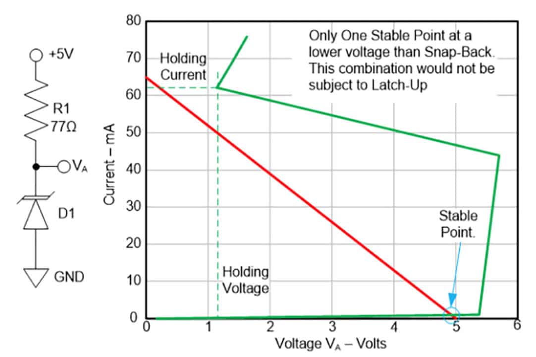
Latch-up can be avoided with proper design. All that needs to be done is to ensure the second and third crossing points do not exist by careful selection of either pull-up resistor or the protection devices holding current and voltage.
Other Considerations
Board Layout
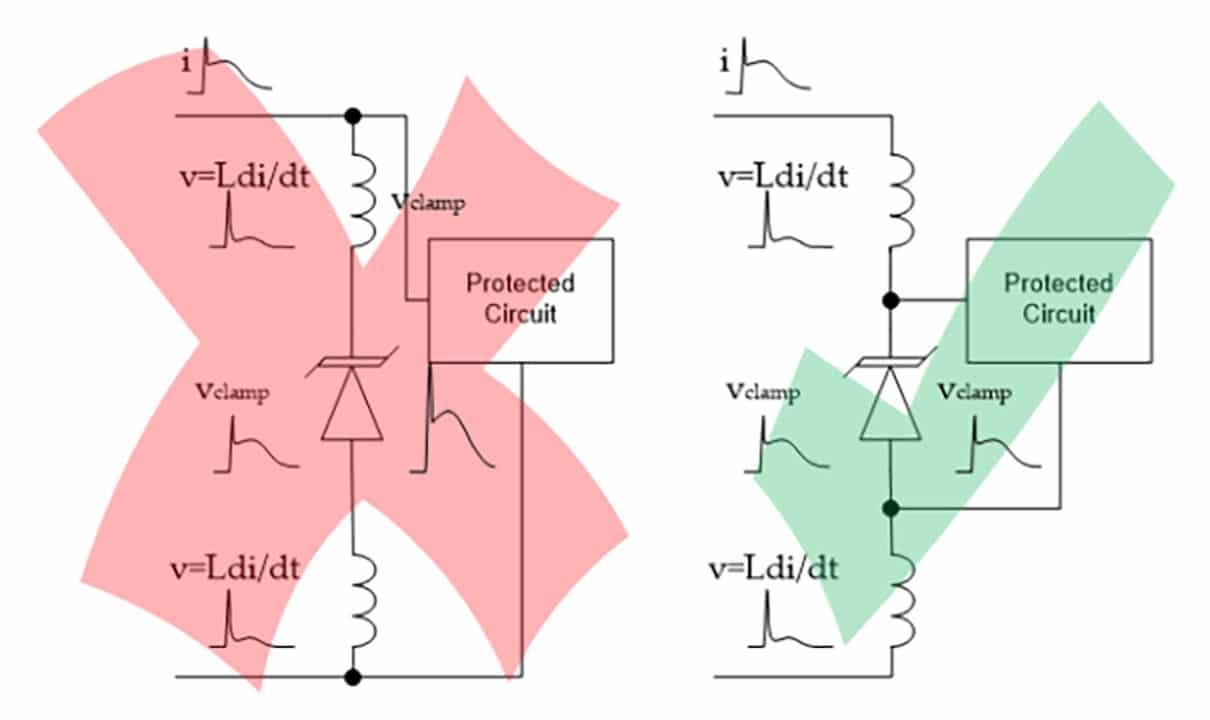
The best protection device in the world will not be able to do its job properly if the board layout is not optimum. Guidelines for proper board layout include: 1. Protect at the system input, i.e. generally, the protection device should be as close as possible to the connector where any transient event might be injected. 2:. Use Kelvin like connections to avoid adding spikes due to parasitic inductance (Figure 8).
3. Minimize any opportunities for coupling. Avoid routing the protected circuitry close to the protection circuitry. Take care with ground planes to ensure return currents are properly controlled. Minimize loop areas to minimize radiation, pickup and inductance, a good practice in any case.
Multi-Line Protection
Multi-line protection packages are becoming more popular and are generally tailored for a particular application. Of course, the packages are larger and generally have slightly higher inductance than an equivalent single line package. Make sure that this extra inductance will not be detrimental in the intended application. The insertion loss curves in the part datasheet will be helpful here. If possible, the signal lines should be made to “flow through” without major directional changes to help maintain proper signal integrity.
Summary
By using a systematic approach, it is relatively straightforward to choose an optimum protection device for a given application by using knowledge of the system and the detailed protection requirements. In most cases, the application is well known and the protection device manufacturer will have a sub-set of their devices already chosen for the application. This will be a good starting point for protection device selection.
References
- Digital Communications, Andy Bateman, Addison-Wesley 1998, ISBN 0-201-34301-0.
- Signal and Power Integrity – Simplified 2nd Ed, Eric Bogatin, Prentice Hall. 2010, ISBN 0-13-234979-5.
- Snap-Back TVS and Load Line Analysis. Dave Rose, Semtech Internal Presentation.
- TVS35-TVS Technology Theory and Comparison; SCR vs. EPD vs. TVS Diodes. Dave Rose, Semtech Internal App Note.


