Abstract
Worst-case Cable Discharge Events (CDE) are poorly understood by most of the product developers as the definition of what is about to happen when you plug in a cable into an appliance’s socket. It is NOT the electro-static charge which could be expected on the cable: outer/inner shield(s) + internal wires, while the cable is fully floating prior to the cable insertion but the total charge which could be on the cable while it is connected to another appliance at the far-end prior to insertion onto a device under test (DUT) port.
Introduction
With further integration and miniaturization of electronics into appliances e.g. Internet of Things (IoT), the use of supply and communication ports, both wired and wireless, with these appliances is increasing rapidly. Accordingly, the occurrence of plugging-in ‘charged’ cables into appliances is likely to increase too. The order in which we make these connections is fully random i.e. we can first connect the low-voltage appliance to the AC/DC plug and then connect it into the public mains wall outlet, or we connect the AC/DC plug into the wall outlet first and then connect the DC plug into the appliance. The same applies to any other cable to be connected to the appliances to be connected while loaded at the far-end.
W.r.t. cables, either shielded or non-shielded, an induced ‘electrostatic static’ charge on the cable (in any way) will be canceled out in-between the shields and inner wires such that the entire cable will become charged as a whole towards the outer environment. Most sockets on appliances, like USB, HMDI, have a protruding outer shield contact terminal which will discharge most of the ‘static’ cable charge through a path alongside the more vulnerable electronics.
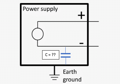
Figure 1: Floating DC output with an undefined capacitance to PE i.e. earth ground
What is less understood is that many electronic devices i.e. appliances are DC-wise at their low-voltage electronics side separated from the protective earth (PE) with class I electric and electronic devices or fully insulated (double or re-enforced) with class II electrical devices. With class II electric devices the maximum capacitance between the primary mains side and the secondary touchable low voltage DC-side is limited, for the sake to satisfy electrical safety requirements like touch voltages and touch currents, to 5 nF. No bleeder resistance is added in parallel, so nearly any voltage can be expected up to a (electrical safety test) minimum of 3 kV. With electrical class I power supplies (with PE terminal), either desktop, AC/DC power plugs or build-in modules, AC/DC desktop power supplies, the inner capacitance in-between the floating DC port and the PE terminal is unrestricted and can be as high as 100 nF. No bleeding resistance is typically added in parallel, so nearly any voltage can be expected up to a (test) minimum of 1,5 kV (that this insulation barrier has to be able to withstand for 1 minute).
According to ‘good engineering practice’ the outer shield of a socket to a (shielded) cable will be connected to the shield of the appliance, either external metal or internally e.g. with laptops and displays as where the inner signal reference i.e. signal ground and/or ‘0 volt’ may be kept insulated from one another as there is NO electrical design requirement nor electrical code which requires, at the low voltage side, that these two: signal ground and PE, have to be connected i.e. electrically short-circuited. The physical insulation barrier between the outer shield and the inner pins of the socket and connector and will be limited to the insulation distance: creepage/clearance, in-between and as such will limit the maximum voltage to which the charge build-up may occur to typically less than 1 kV.
CDE testing using a TLP generator
Rather than using a large variety of cable configurations and far-end terminations to show the appliance’s port withstand capabilities against the above-described phenomena, a standard TLP generator [1,2] can be used which has options to add near-end and far-end termination networks externally to the internal 50 Ω charged cable system provided. As an example, when a standard TLP is converted to an HMM source [3], an HMM-network is added at the near-end of the TLP generator output to adapt the TLP generator to become a conductive system level ESD source which can generate short-circuit currents equal to those as generated by an IEC 61000-4-2 ESD gun.
By adding a lumped capacitance network at the far end of the internal charged cable system provided in the TLP source, a condition equal to the far-end loaded cables can be generated. Dependent upon the common-mode characteristic impedance between the inner wires i.e. inner shields against the outer shield, an impedance matching needs to be provided. The common mode impedance between internal wires to outer shield impedance varies between 20 to 50 Ω. Inner shields to outer shield characteristic impedances can be less than 10 Ω.
Different from the initial pulse as occurring with the HMM-pulse, an extra trailing pulse will result at the end of the TLP pulse in the CDE approach. The pulse duration (= twice the cable length propagation) and the equivalent characteristic impedance, as required to emulate the charged cable event as intended worst-case, needs to be applied to the socket pins versus the outer shell of the appliance port under test.
As can be seen in the figures 2 and 4, the equivalent circuit diagram is straight forward and the circuit parameters are determined by the geometrical details of the cables used and the far-end loads to be expected.
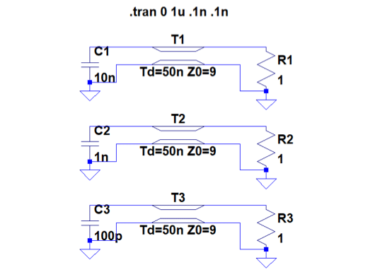
Figure 2: CDE TLP test setup, Z0= 9 Ω, with various far-end load conditions
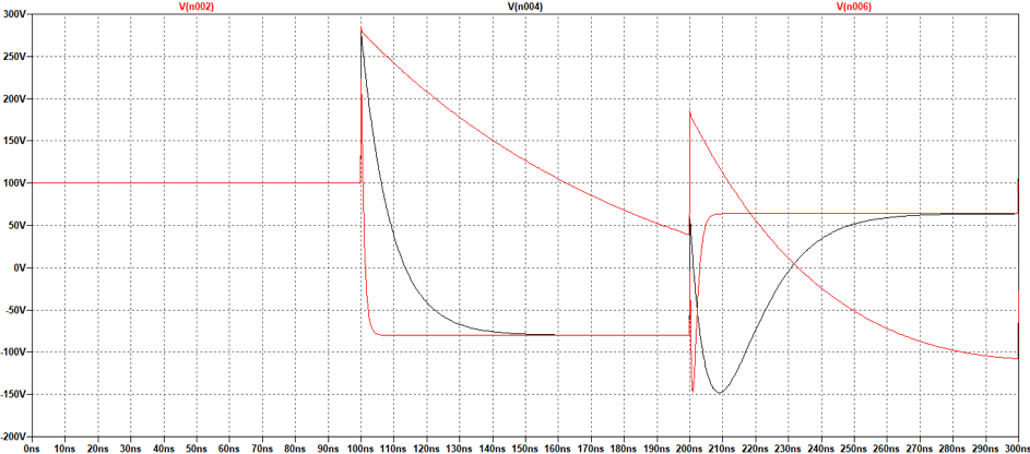
Figure 3: Discharge current waveshape: a generic TLP pulse of 100 ns (Z0 = 9 Ω !!) @100 Amps followed by the CDE ‘afterburner’ @ 280 Amps peak represented by the far-end loads when charged to 1 kV.
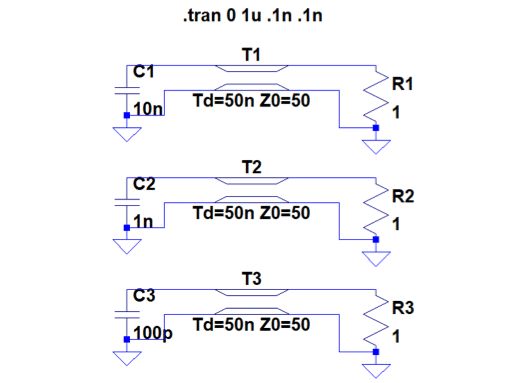
Figure 4: CDE TLP test setup, Z0 = 50 Ω, with various far-end load conditions
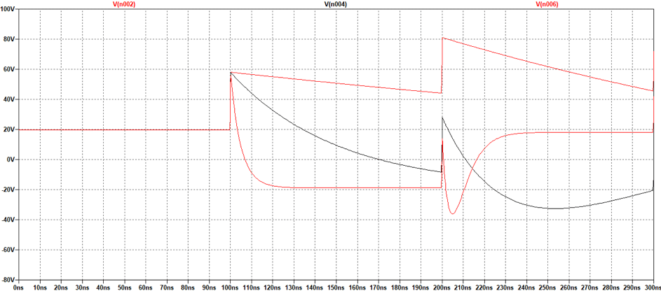
Figure 5: Discharge current waveshape: a generic TLP pulse of 100 ns (Z0 = 50 Ω!!) @ ~20 Amps followed by the CDE ‘afterburner’ up to 80 Amps peak represented by the far-end loads when charged to 1kV.
As can be seen from figure 3 and 5, the ‘burden’ of the discharge stress is in the tail of the CDE pulse as presented by a modified TLP pulse generator. The common-mode characteristic impedance, 1 kV charged cable will be initially current limited by the characteristic impedance of the transmission line and the near-end load impedance. The trailing pulse decay time is given by the RLC time constant of the far-end capacitance and the load resistance and the equivalent inductance of the cable.
With different transmission line topologies, three main common mode impedances shall be considered: 150 Ω being the common mode impedance for non-shielded cables, 50 Ω for multi-wires inside an outer shielded cable and ~ 10 Ω for an inner-shielded cable against the outer shield. The TLP pulse length taken shall be related to the worst-case i.e. maximum length condition as specified e.g. USB-2: 5 meter, HDMI: 15 meters, Ethernet 1 Gb/s: 57 meters.
Conclusions
With worst-case CDE testing, the peak discharge currents will, by the far-end load, exceed the 50 Ω TLP test conditions by a factor 3 – 14 and will last substantially longer (compared to the standardized 100 ns TLP pulse). As such compliance to the TLP requirements at pin or port level will not guarantee a non-failure for a worst-case CDE occurrence for the port interface of the appliance concerned.
With COTS AC/DC supplies, varying from low-power USB device chargers to desktop power supplies and built-in power supply modules, and as such with most secondary insulated electronic circuits, capacitances between ~30 pF till 100 nF have been found without any bleeder resistances in parallel to the primary PE side, i.e. the charge voltages will be undefined.
Voltage differences between the inner wires, inner shields and/or outer shields of a non-far-end terminated cable will diminish in short time and the cable as a whole will appear charged against the outer environment but will not result in the severe stress condition as given above. This cable discharge condition will be solved by the protruding contacts for the outer shield at the socket. The protruding ground connection with the socket will NOT prevent the overstress from the worst-case CDE stress as given above.
Bibliography
Mart Coenen runs its business as an independent consultant for 25 years and is since 40 years involved in EMC and ESD matters. Since 1988 he is involved in IEC and CENELEC international standardization. In 2013 he became involved in ESD as member of the ESDA where he cooperates together with most IC manufacturers and electronic product manufacturers.
References
[1] ESD TR5.5-01-08, ESD Association Technical Report for the Protection of Electrostatic Discharge Susceptible Items – Transmission Line Pulse (TLP)
[2] ESD TR5.5-04-18, ESD Association Technical Report for Electrostatic Discharge Sensitivity Testing – Transmission Line Pulse (TLP) – User and Application Guide
[3] ESD TR5.6-01-09, ESD Association Technical Report for the Protection of Electrostatic Discharge Susceptible Items – Human Metal Model (HMM)
[4] ANSI/ESD SP5.6-2009, ESD Association Standard Practice for Electrostatic Discharge Sensitivity Testing – Human Metal Model (HMM) – Component Level
