INTRODUCTION
One of the roles of the practicing EMC engineer or product designer is to be able to design filters to add to circuits in order to get them to pass various EMC immunity and emissions standards such as IEC 61000-4-2 for ESD immunity, IEC 61000-4-3 for Radiated RF immunity and IEC 61000-4-4 for Electrical Fast Transient/Burst immunity and other various international standards covering Radiated Emissions (RE) or Conducted Emissions (CE).
EMI filters are often used along with proper shielding in order to achieve EMC compliance. The purpose of a filter is to establish either a low-impedance path for RF current to return back to the local source of energy, and/or to provide a high impedance to prevent RF currents from flowing on a cable. However, selecting the proper filter for a given situation may be confusing to some, especially if they are new to the EMC field or have not dealt with the subject in some time.
EMC practitioners may be asking themselves what filter configuration is the best one to use for any given application or how to correctly choose the values of components given the frequency, circuit impedance, and other parameters of the circuit. They may also want to know how they can get more attenuation out of their filter design in order to pass an emissions or immunity test. The time to learn how to properly design filters for EMC compliance is not when schedules are tight, and the product’s ship date is rapidly approaching.
If you find yourself stuck in any of the above situations, this article on passive filter basics for EMC compliance should help remove the mystery, and allow you to quickly find the best passive component filter solution that allows product to ship on time.
BASICS OF PASSIVE FILTERS FOR EMC COMPLIANCE
PASSIVE LOW-PASS FILTERS
Fortunately, designing filters for EMC compliance is not as difficult as it may seem. For most cases, in order to achieve EMC compliance, we really only need to know how to apply passive low-pass filter types to our circuits. The other types of passive filters, such as high-pass,
band-pass, and band-reject are not as common as the low-pass filter is for EMC work and will not be covered in this paper. Consult the references for more information on these other filter types.
Unfortunately, circuit impedances are not always well understood or impossible to know, making it more difficult to determine which values of passive low-pass filter components to choose from in order to pass the EMC compliance tests. This is the situation with common mode emissions emanating off of a cable during a RE test where the impedance of the cable changes as it is rearranged in order to maximize emissions (Reference [1]).
It is impossible to model the filter exactly if the load impedance is not known. The only way to know if a lowpass filter design is adequate or not is by trial and error experiments performed during EMC compliance testing, or more preferably, by trying out different low-pass filter
component values very early in the product development cycle. In order to be most effective, this experimental work should occur during pre-compliance testing performed in your own test facility prior to going out of house for full-compliance testing. See Reference [3] for a detailed description on how to setup an in-house pre-compliance EMC test facility.
A low-pass filter is one in which the frequencies below a certain significant frequency are easily let-through and those above this same significant frequency are heavily attenuated. A passive low-pass filter is a simple voltage divider; non-amplifying device composed of a combination of resistors and capacitors, inductors (or ferrites) and capacitors or in some instances, may be composed of just one of these components. For instance, a single capacitor placed across a line to reference ground without the resistor or inductor installed may be all that is required in order to suppress an unwanted signal.
The benefit to using a single component filter is that only one physical device is required which in turn requires less board space and also helps keep parts costs down. Multi-element filters are useful in situations where the range of frequencies involved is too large and impossible
for a one component filter to fully attenuate.
RC LOW-PASS FILTER
One of the most basic forms of a low-pass filter is comprised of just one resistor and one capacitor, an RC filter. In an RC low-pass filter, the cutoff frequency occurs at resonance, where the capacitive reactance (Xc) equals the resistance (R) and where Xc =1/2πfC (Reference [4]).
A simple RC low-pass filter and the equation for determining its cutoff frequency is shown in Figure 1. Note that the filter shown in Figure 1 is also known as an L filter due to its resemblance to the letter L. It is also considered a single-pole filter because there is only one reactive component, the capacitor.
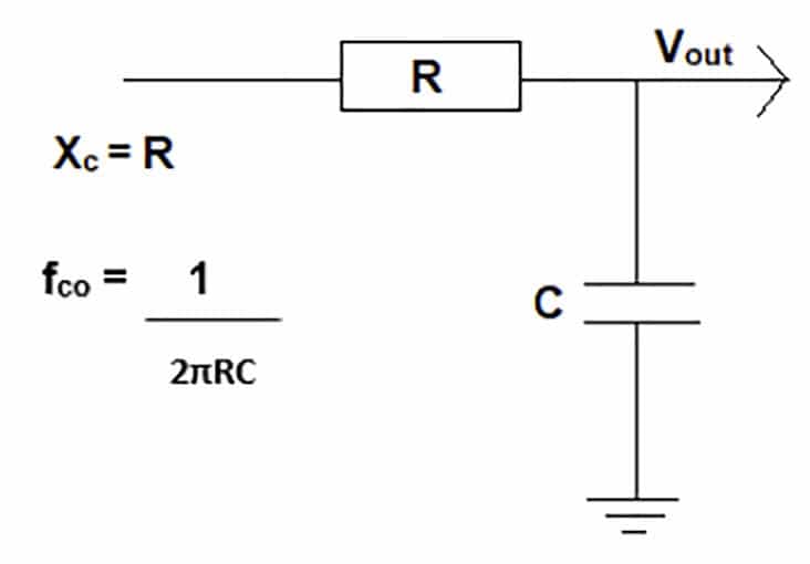
Figure 1: Basic RC Low-Pass Filter (L Type)
A low-pass filter has an ideal, theoretical response where all signals contained below a so-called critical frequency (the 3 dB down point) are easily let-through the device and above which frequency, all signals are heavily attenuated. An ideal low-pass filter response curve is shown in Figure 2.
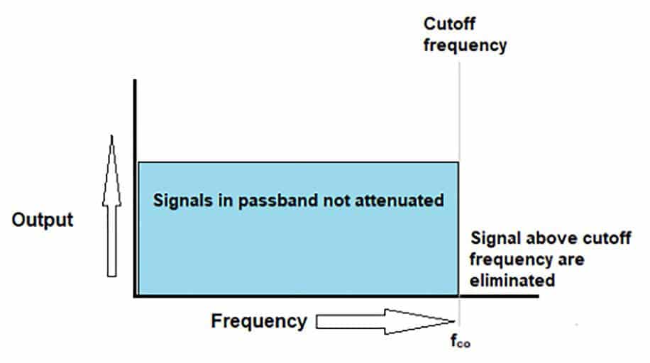
Figure 2: Ideal low-pass filter response curve
In actual practice, the output of the filter will not go to zero as abruptly as shown in the ideal curve of Figure 2. In actuality, the output will gradually roll off at a 6 dB/octave or 20 dB/decade rate as shown in Figure 3.
EMC APPLICATION OF LOW-PASS FILTERS
Reference [3] suggests applying a low-pass filter in order to fix an EMC problem such as a fast transient or ESD discharge immunity issue and that a good starting point in putting together a low-pass filter that will work for most situations is to start out by using a 47 to 100Ω series resistor placed in the signal line, with a 1 to 10nF capacitor placed in the signal or power return line. If we take this information and select R = 100Ω and C = 10nF as a starting point, the cut-off frequency (fco) will equal approximately 159 kHz, and the low-pass filter response curve should look like that shown in Figure 3. Very little of the signals that are greater than 1.59 MHz will be let through the filter
as they are 20 dB lower than any of the signals that at the filter’s cutoff frequency of 159 kHz.
As another example, if we leave R = 100Ω and select C = 1nF, the cutoff frequency at the 3 dB down point moves out to roughly 1.59 MHz, the 6 dB down point is at 3.2 MHz, and the signal is almost completely attenuated at 15.9 MHz. Signals greater than 15.9 MHz are heavily attenuated and not let through the filter.
Table 1 contains a matrix of the various R-C low-pass filter values discussed so far plus some others that might be useful, and their low-pass filter characteristic responses at the 6 dB and 20 dB down points.
When attempting to suppress an unwanted high-frequency signal, one may find out that a filter containing only a single reactive component (i.e. one capacitor or one inductor) may not provide enough attenuation. Adding a second reactive component will increase the roll off to 12
dB/octave or 40 dB/decade (Reference [4]). These types of filters are called various names such as double-pole, two-stage, two-element, or second-order filters. Filters with three reactive components will provide 18 dB/octave or 60 dB/decade attenuation. Four reactive component filters will provide 24 dB/octave or 80 dB/decade attenuation and so on (Reference [2]).
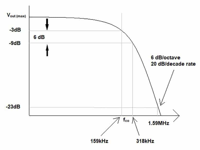
Figure 3: Realistic low-pass filter response curve
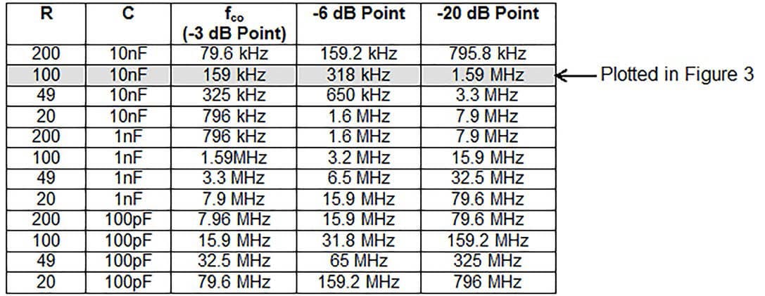
Table 1: Matrix of R-C Values and Low-Pass Filter Responses
SELECTION OF FCO
When selecting a cut-off frequency for a low-pass filter, it is important to take into account the fundamental frequency of the intended data, clocks, and other purposeful signals present on the filtered line. If the cut-off frequency chosen is too low in frequency, then the intended signals will be attenuated along with the higher frequency signals that you want to suppress. Try to maintain at least the 5th harmonic of the intended signal, with the 10th harmonic being ideal (Reference [3]). Many I/O signals that are used with unshielded cables require some form of filtering in order to be in compliance with EMC standards. These signals usually have a frequency of 1 MHz or less (Reference [1]). It is important to also ensure that by adding a filter’s impedance to circuit that it does not in turn create a signal integrity problem.
Once the filter’s component values are chosen, carefully consider where it is going to be placed in the circuit or system. The most benefit is obtained when the filter is placed as close to the item to be protected as possible, one centimeter is ideal for most designs (Reference [1]).
In order to keep any extra unwanted inductance from affecting performance of the filter, be sure to keep lead lengths as short as possible. Additional layout and placement concerns will be covered later in this article.
USE OF FERRITES
If the voltage drop across the series resistor cannot be tolerated, a device such as a ferrite, which acts as a high-frequency resistor with minimal voltage drop, can be used instead of the resistor. Because the ferrite presents the circuit with high AC impedance, while also not
affecting signal quality, they are most optimal for filtering at frequencies greater than 30 MHz. Carefully consider the amount of DC or low-frequency current present in the circuit when using ferrites. They can become easily saturated with too much current present in the circuit which renders them ineffective (Reference [5]).
USE OF INDUCTORS
An inductor can also be considered for the series element in a low-pass filter instead of a resistor or ferrite, particularly if dealing with a signal in the 10 to 30 MHz range. When using inductors, beware of the effect that their inductive reactance (XL = 2πfL) and parasitic capacitance will have at these higher frequencies. You may be actually creating a high-pass filter when you are attempting to create a low-pass one, and not even realize it.
BASIC FILTER TOPOLOGIES
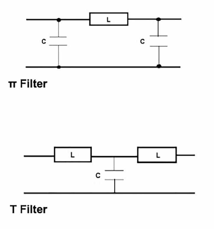
The following diagrams show two more of the basic filter configurations available for impedance mismatching between circuit source and load input and output impedances and filter input and output impedances. Both are named after their shapes. The first is called a π filter because it looks like the Greek letter π and the second is called the T filter because it looks like the letter T. Note that there are three reactive elements present in these filters which means they an attenuation curve of 18 dB/ octave and 60 dB/decade. They are considered third-order filters (Reference [5]).
IMPEDANCE MISMATCHING
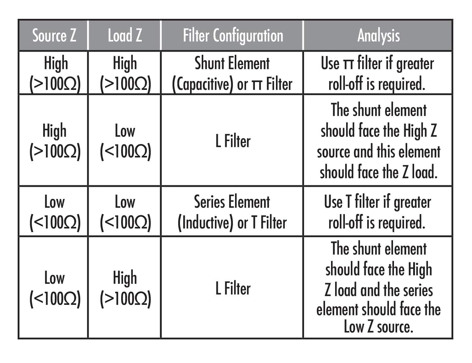
Source and load impedances must be considered in selecting the proper filter configuration. If order to work properly, the source driving the input to the low-impedance shunt element (i.e. capacitor), should be a high-impedance. If the output of the source is a low-impedance, it should face the high-impedance series component. This same concept applies to load input impedances versus the filter’s output impedances. In general, a source or load impedance less than 100 Ω is considered low and great than 100Ω is considered high impedance (Reference [5]). Table 1 provides a matrix of source versus load impedances and their associated correct filter topologies.
DIFFERENTIAL MODE (DM) AND COMMON MODE (CM) CURRENTS
There are two different types of current modes, and hence noise sources capable of creating interference. It is important to know which mode is prevalent so that proper filtering can be applied. The two types of signals we are referring to are differential mode (DM) and common-mode (CM) signals.
DM signals carry useful information whereas CM currents provide no useful information what-so-ever and are the main source of RE and CE issues. A DM signal travels down one side of a circuit path, and an equal and opposite DM signal travels back on the other side of the path. If no circuit discontinues exists, then complete canceling of these two DM signals occur, and no CM current is developed. Placing capacitors across the outgoing and return lines and/or an inductor in series with either outgoing or return line is called DM filtering.
CM signals are in-phase signals present in both outgoing and return lines of a circuit. They do not cancel each other out but add up, often to a level substantial enough to cause EMI issues. CM filtering involves placing capacitors across each signal line to ground reference and sometimes also using a CM inductor in the circuit. The CM inductor only acts on the CM signals that are present. It does not affect the DM signals.
PARASITICS
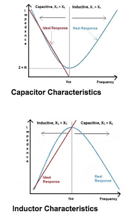
The non-ideal behavior of the elements that make up our filter must be addressed. Unexpectedly, we will find that real capacitors and inductors possess both capacitance and inductance which limits the bandwidth that they are useful over. The amount of parasitics present in a circuit can be reduced through proper component selection and layout techniques, but cannot be eliminated entirely. As frequency increases, the reactance of a capacitor decreases until it reaches its self-resonant frequency. Up to this point, the capacitor is behaving as it should – it behaves like a resistor. Above its self-resonant frequency point the capacitor becomes inductive and it acts like an inductor because of the parasitic inductance found in its metal plates. This parasitic effect is greater in leaded types of capacitors than it is with the surface mount technology (SMT) types that have almost no lead length.
The opposite effect occurs with an inductor where its reactance becomes capacitive above its self-resonant frequency point, and where the inductor now acts like a capacitor. At the self-resonant frequency, capacitors are intended to provide a very low impedance and inductors
should provide a high impedance. For inductors, their limiting factors are related to the parasitic capacitance present between each winding and overall capacitance located between one lead and the other.
The inductor’s inter-winding parasitic capacitance is not as big a deal in regards to effectiveness for EMI suppression as is a capacitor’s parasitic inductance. The main factors that change the intended behavior of capacitors is the parasitic inductance of the circuits in which they are installed, not necessarily the construction of the capacitor. Therefore, proper layout and placement then becomes the critical factor when attempting to effective utilize passive low-pass filters for EMI suppression.
LAYOUT AND PLACEMENT CONCERNS
Because there is going to be unknown and hidden parasitics involved, do not expect your filter design to work one-hundred percent the first time. As mentioned earlier, expect the need to perform some trial and error design and troubleshooting in the lab. If not available already, have on hand a selection of various components that you want to try out. Do not wait until the last minute to obtain the SMT capacitors, inductors, or ferrites that you want to use. Make sure the components selected are designed for the bandwidths involved. Create your own matrix of values, critical frequencies, and 6- and 20-dB roll-off curves.
In reviewing the layout, look for longer than necessary trace lengths that add extra inductance and impedance. When applying fixes, be sure keep connections short. If an R-C filter is added to the reset pin of a micro-controller, place it as close to the pin as possible and do not overlook the length of its return trace. In general, it is best to locate the filter as close to the offending signal source as possible, not some obscure location far away.
Watch out for trace or wire routing that allows for too much capacitive and inductive coupling to other noisy signal or traces. Filter components should be placed right at an entry connector (I/O and power inputs). Placement of a filter deeper inside a circuit or system allows EMI to enter the system (Reference [6]). If separation is not maintained, improper routing of input and output sections can mean that filter elements are essentially bypassed and no longer effective. On PCBs, capacitors should shunt unwanted signals to chassis not line to line or line to return (Reference [6]). It is best to understand the path of current flow and to not necessarily rely on “ground” as being the ultimate zero-ohm impedance and sole problem savior.
Finally, although they appear to be useful and easy to troubleshoot with, do not expect too much out of clampon ferrite common-mode chokes as they only provide about 10 dB of attenuation (Reference [3]).
CONCLUSION
The need to utilize passive low-pass filters to obtain EMC compliance is a given. They provide a low-impedance path for RF currents to return back to the local source of energy or provide a high impedance to prevent unwanted RF currents from flowing. A filter that does both is ideal. Designing low-pass filters for EMI suppression is not that difficult. Proper knowledge and planning before the need for them arises can save developers some time and headaches.
REFERENCES
[1] Archambeault, PCB Design for Real-World EMI Control, Kluwer Academic Publishers, 2002
[2] Frenzel, Jr., Principals of Electronic Communications Systems, Fourth Edition, McGraw-Hill, 2016
[3] André & Wyatt, EMI Troubleshooting Cookbook for Product Designers, Scitech Publishing, 2014.
[4] Montrose, EMC Made Simple, Printed Circuit Board and System Design, Montrose Compliance Services, Inc., 2014
[5] Armstrong, EMC Filters Guide, Interference Technology, 2017
[6] Montrose, Printed Circuit Board Design Techniques for EMC Compliance – A Handbook for Designers, 2nd Edition, 2000.
