As a consultant, I’m seeing an increasing number of manufacturers wanting to add or retrofit wireless into new or existing products. Products typically include mobile, household, industrial, scientific, and medical devices. Also, the trend toward the “Internet of Things” (IoT) or the Industrial Internet of Things (IIoT) adds to the problem. This transition towards “everything wireless” is in full swing and with it comes problems with EMI. That is, EMI from the product itself interfering with sensitive on-board telephone, GPS/GNSS, and Wi-Fi/Bluetooth receivers. This is called “platform” or self-interference and it’s a big problem for manufacturers.
Most digital-based products create a host of on-board radio frequency “noise” (electromagnetic interference, or EMI), that usually won’t bother the digital circuitry itself, but the harmonic energy from digital clocks, high-speed data buses, and on-board switch-mode power supplies can easily create interference well into the 700 to 950 MHz mobile phone bands, causing receiver “desense” (reduced receiver sensitivity). In order to use the various mobile phone services (Verizon, ATT, Sprint, T-Mobile, and others in the U.S.), manufacturers must pass very stringent receiver sensitivity and transmitter power compliance tests, as described above, according to CTIA standards. This on-board digital noise often delays product introductions for weeks or months.
Cellular and wireless providers require a certain receiver sensitivity in dBm called Total Isotropic Sensitivity, or TIS. For example, this might typically be a sensitivity of -108 dBm, and must include the effect of antenna efficiency used in the mobile device. Because mobile device antennas typically operate in close proximity to human hands or head, this tends to reduce the sensitivity further (-99 dBm might be typical, depending on the antenna). More information on this, as well as the test methods, are described in “Test Plan for Mobile Station Over the Air Performance: Method of Measurement for Radiated RF Power and Receiver Performance“, by the CTIA (Cellular Telephone Industries Association), now known as “CTIA – The Wireless Association”. See Reference 1. Cellular radio manufacturer, Broadcom, also has some information in their white paper, Compliance with TIS and TRP Requirements (Reference 2).
Several recent clients all had platform interference issues that kept their products off the market for weeks or months until major product redesigns were done. In this article, I’ll show what this noise looks like, how to measure it, and will list common problem areas and suggest some mitigations.
Characterizing On-Board Noise (Platform Interference)
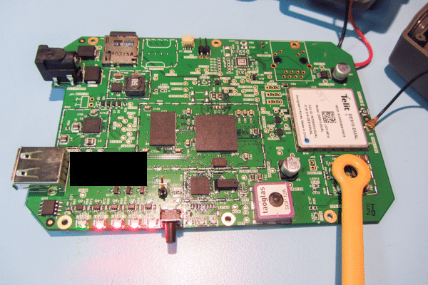
First, let’s take a look at a typical product. Specific details will remain general for confidentiality purposes. This board includes a USB port whose data ultimately gets transmitted via various mobile phone systems, depending upon the factory configuration.
There are generally two primary areas of focus where on-board noise can couple to the receiver antenna and cause receiver degradation:
- On-board sources, such as DC-DC converters, address and data buses, and other fast-edged digital signals
- Attached cables that act as “radiating structures” (antennas), such as I/O and power cables
There are two measurement techniques I commonly use to characterize platform interference
- High frequency current probes are best used for measuring small RF currents on cables
- Near field magnetic or electric field probes for locating noise sources
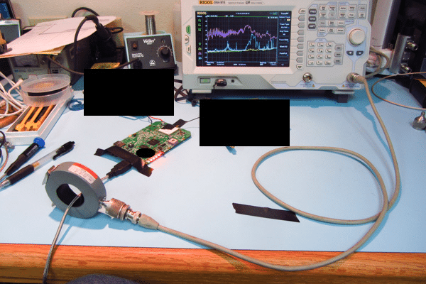
In Figure 1 below, a current probe is used to measure the common mode harmonic currents flowing on the outside of a shielded USB cable. How these currents are formed and why they tend to couple onto cables is explained more completely in References 2 and 3. Let’s just say that noise currents generated on the PC board can easily couple to attached I/O and power cables.
The spectrum analyzer is the most useful tool for these measurements, as entire frequency spectrums may be observed. Figure 1 shows the general test setup.

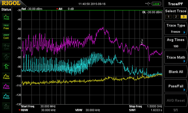
There are two common types of high frequency harmonic plots; narrow band and broadband. Figure 2 shows the difference as we’re looking from 9 kHz to 1.5 GHz. Typically, DC-DC converters or data/address bus data will appear as a very broad signal with several resonant peaks (violet trace in Figure 2), while crystal oscillators or high speed clocks will appear as a series of narrow spikes (aqua trace in Figure 2). Unless the product is designed for EMC compliance, both these types of signals can radiate or conduct high frequency energy well into the mobile phone bands.


Types of Measurements
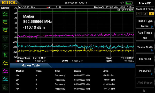
There are generally two types of measurements I suggest performing. The first helps characterize the general profile of noise sources, such as DC-DC converters, clock buses, processors, RAM, and any other potential high frequency device. This measurement is taken from least 1 to 1000 MHz, in order to characterize the general spectral profile and to see whether any energy extends into the receiver passband of concern (Figure 4). For other mobile phone and/or GPS/GNSS, you’ll need to look as high as 2 GHz. For Wi-Fi, you’ll need to look as high as 2.5 or 5.4 GHz. Placing the spectrum analyzer in “Max Hold” mode is used to build up a maximum spectral amplitude.

Once the various noise sources on the board are identified, the next measurement I suggest is to look at just the receiver (downlink) band. In the case of Verizon in the U.S., for example, this would be “Band 13” of the FCC allocation from 746 to 756 MHz. You’ll probably need an external broadband preamplifier of at least 20 to 30 dB gain in order to clearly observe the noise, if any. I generally turn on the 20 dB built-in preamplifier in the analyzer, as well. The Beehive Electronics Model 150A external amplifier, with frequency range of 100 kHz to 6 GHz, works well, but there are many other companies, such as Aaronia, TekBox, Com-Power, Rohde & Schwarz, and Keysight that sell high-gain broadband preamplifiers with low noise figure. You’ll probably need to make these measurements inside a shielded room in order to exclude other mobile phone transmissions from disrupting your measurements. An examples are shown in Figure 5.

Remediation Checklist
As I mentioned, the product design must be developed with EMC in mind and no corners should be cut. This will consist of:
- A near perfect PC board layout
- Filtering of DC-DC converters
- Filtering of any other high frequency device
- Filtering at the radio module
- Local shielding around high noise areas
- Possibly shielding the entire product
- Proper antenna placement
The PC board layout is critical and is where most of your effort should be spent. An eight or ten layer stack-up will provide the most flexibility in segregating the power supply, analog, digital, and radio sections and provide multiple ground return planes, which may be stitched together around the board edge to form a Faraday cage. Care must be taken to avoid return current contamination between sections (common impedance coupling). According to Reference 5, isolating the power plane for the radio section from the digital power plane (except for a narrow bridge) can provide up to 40 dB of isolation between the digital circuitry and radio.
It is vital that the power and ground return planes be on adjacent layers, and 3-4 mils apart, at the most. This will provide the best high frequency decoupling. Clocks, or other high speed traces, should avoid passing through too many vias and should not change reference planes.
DC-DC power supply sections should be well isolated from sensitive analog or radio circuitry (including antennas). Be aware of primary and secondary current loops and their return currents. These return currents should not share the same return plane paths as digital, analog, or radio circuits. remember that return currents above about 50 kHz want to return directly under the source trace.
For general product design guidelines, the books, EMI Troubleshooting Cookbook for Product Designers, by Patrick André and Kenneth Wyatt and Electromagnetic Compatibility Engineering, by Henry Ott (References 3 and 4), describe several basic design concepts to reduce EMI. Platform Interference in Wireless Systems, by Intel engineers, Kevin Slattery and Harry Skinner, is very useful in providing ideas for measurement and remediation (Reference 5).
Summary
Platform interference has quickly become one of the most challenging issues for manufacturers building in wireless technology into new or existing products. Success depends on carefully designing the entire product to ensure minimal EMI. Proper circuit board layout and stack-up is a key factor for success. Cutting corners by simply “bolting on” a cellular modem to an existing product is a recipe for disaster.
References
- CTIA, Test Plan for Mobile Station Over the Air Performance: Method of Measurement for Radiated RF Power and Receiver Performance, http://files.ctia.org/pdf/CTIA_OTA_Test_Plan_Rev_3.1.pdf
- Broadcom, Compliance with TIS and TRP Requirements, https://www.broadcom.com/collateral/wp/21XX-WP100-R.pdf
- André and Wyatt, EMI Troubleshooting Cookbook for Product Designers, SciTech Publishing, 2014.
- Ott, Electromagnetic Compatibility Engineering, Wiley, 2009.
- Slattery and Skinner, Platform Interference in Wireless Systems – Models, Measurement, and Mitigation, Newness Press, 2008.


