Mart Coenen
For many years national and international norms and standards have been established to make device and product design and manufacturing life easier or at least defined within bounds. In most cases, there is even a life-cycle process for the norms and standards themselves. Old ones fade away and new ones flourish, but some remain everlasting though new insights have proven otherwise. The standardization processes are to create references and stability or to set long lasting trade barriers. Test equipment manufacturers, test houses and industry want an economic return on their investments w.r.t. international standard development, test equipment development, and the accompanying constraints all these requirements have on the products and devices that have to adhere these established norms and standards.
Abstract
Changing design requirements has a huge impact on product and device developments in electronic industries. But what if standardization is lagging behind and the requirements posed are no longer suited for the problems occurring in the end-user’s playing field. True, every requirement one changes or poses on product and device developments has an impact of the manufacturing processes chosen, the design effort, the verification method and all other requirements along the development chain up onto the end-users environment (which can hardly be changed and has to be taken as ultimate end-user requirement).
With System-Efficient ESD Design (SEED, see ESDA White Book 3), the ESD performance of nanoscale devices needs to be complemented by additional protection measures to meet the end-users environment. At the device level, the Human Body Model (HBM) or Charged Device Model (CDM) is used. The Machine Model (MM) has formally been abandoned. The Transmission-Line test Method (ANSI/ESD STM5.5.1-2008, IEC 60749-26TLM), typically 100 ns duration or even very fast Transmission-Line test Method (ANSI/ESD SP5.5.2-2007, vf-TLM), typically less than 10 ns duration, is promoted heavily but no quantitative requirements have been posed similar to the HBM and CDM or end-user levels (IEC 61000-4-2).
Due to further miniaturization and thinner gate and insulation oxides with devices, the ESD requirements posed on these devices have to be reduced accordingly as physical limits w.r.t. peak current densities and peak field strength levels across insulating materials are exceeded into the hot electron effect region. As such, supplementary ESD protection requirements have to apply to the production, manufacturing, handling and assembly area as ESD Protected Area (EPA) requirements have to become tighter by two or more classes: IEC 61340-x-y or ANSI/ESD S20.20.
An integral approach is needed along the entire semiconductor device production chain, from wafer grinding to expose, dicing, bonding, assembly, testing, handling and storage to meet those new ESD protection demands which go beyond the ANSI/ESD S20.20. To verify these measures along the production chain up until the end-user environment, new requirements and environmental test methods have to be defined and new reference data bases with strong evidence have to be build (and that is where the harvesting (= less defects) can be started).
Introduction
The ‘old’ ESD test methods for devices stem from the ‘old’ Mil-Std 883 with multi-ns rise-times. The requirements were limited at those days by the measurement bandwidth limitations of oscilloscopes and transient recorders, similar to the ‘old’ product requirements of the IEC 801-2 (1984). In the meanwhile, the end-user ESD requirements have been updated to the IEC 61000-4-2, 2008, representing the touch with a finger by a standing person. The rise time for end-user ESD pulses are in the sub-nanoseconds range: 0,7 – 1 ns followed by a more energetic lead pulse between 30 – 60 ns after initial touching. Further investigations are ongoing which show that metal-to-metal discharges will only be in the tens of picoseconds rise-time. Device level testing has been upgraded accordingly using the CDM test (dropping charged devices on a metal table), also with sub-nanoseconds rise time and short duration.
TLP testing is introduced (1985) as a Panacea tool which can substitute all other ESD pulses up to the end-user requirements. Typically, the TLP method with some waveform shaping networks could do it but the measurement systems as they are commercially provided to the market typically can’t. In particular the fact that the I/V-points are taken after 70% of the pulse width is a matter of ‘seeding’ concern.
System-Efficient ESD Design (SEED)
As defined in the 3rd White Book of the ESDA, the intent is to build an integral ESD protection network in such a way that the ultimate functional circuit is being protected. In principle, this starts at the IC-level where the I/O or supply circuit is protected by the on-chip protection structures. Nowadays, the functional I/O and supply circuits are separately developed by different IP groups and ultimately joined with the pad protection at physical layout.
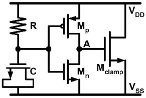
Most ESD protections are typically dV/dt or threshold/ breakdown voltage triggered, see Figure 1. But what if an only dV/dt triggered ESD protection device is used in parallel to a processor core supply circuitry with large equivalent supply decoupling capacitance? The ESD protection circuitry has been characterized separately before it is added to an IP library without considering further application. By the parallel capacitance of the core the dV/dt at the ESD protection circuit is reduced and as the dV/dt in application has become too dull, that dV/dt triggered protection is no longer effective. As such the discharge current occurring with the ESD event charges up the internal core voltage until an overvoltage occurs.
If an external clamping circuit is used which is clamped to e.g. the +5 volt rail while the internal supply voltage of the circuit to be protected is less, then both protections will formally work as intended, but when used in parallel, the external one will have no function as the first voltage rooftop will be reached by the internal supply. Again true, like a tsunami, the external device will do something, but only when it gets triggered in time at its trigger voltage before the internal clamping circuit takes over.
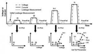
Taking the clamping voltage data from the internal and external protection devices or circuits doesn’t make sense, see Figure 2. Taking the triggering voltage of both devices neither. From both devices, I/V data versus time are required to find out which one takes the burden. As such, taking the I/V data after 70% of the TLP edge doesn’t make sense as the whole transition versus time contains the crucial information, see Figure 3. As TLP systems generate pulses with rise times in the order of 100 ps or even less (≈ 3 GHz bandwidth), the sampling time for the current and voltage data has to be taken even faster considering Nyquist. Furthermore, the two: current and voltage, have to be taken simultaneously with sufficient bandwidth, both for the scope used, as for the sensors, see Figure 4.
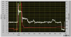
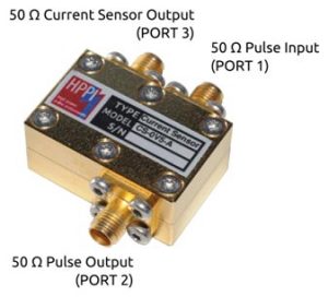
As testing by using (vf-)TLP is artificial w.r.t the real ESD phenomena, it is still debatable on whether the data: I/V versus time, found is practically suitable enough to enable SEED prediction. Again, true … only by having the entire I/V versus time data base will enable a correct input for analogue circuit simulations. Even the inclusion of specific discretized and extracted 3D-layout information of the PCB and IC-packages into this equation is possible.
CDM
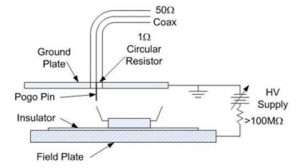
The use of the device charging plate with CDM test method which is not RF-wise defined decoupled to the 1 W sense resistor reference plane doesn’t make sense, see Figure 5. Theoretically, the max. di/dt will be the charged voltage to the device (towards the sense resistor reference plane, not the charging plate) divided by 1 W. In reality, by the commercially CDM test systems offered, the di/dt will be immediately limited by the length of the test (pogo) pin used. As a CDM standard update is in progress between ANSI/JEDEC and ESDA, the critical factors for testing i.e. qualification and quantification shall be identified and restrictions to those parameters shall be given. Otherwise the whole CDM test reduces to a unified test method which, as long as everyone is making the same mistakes, is providing a common relative reference test method rather than an absolute one.
Conclusions
Before one can start to harvest SEED, the seeding and breeding has to take place, which will not occur overnight. But to harvest the right SEED parameters, one needs to adapt the way of measurement and characterization first. The ingredients for artificial ESD measurement by the TLP method are there, but the right application to gather the SEED data correctly is lacking.
The SEED approach doesn’t only apply between ICs and external protection devices but also between on-chip circuits and the I/O and supply ESD protection circuits. When split grounds are used; VSSA, VSSD, VSSX, etc., also here the SEED approach shall be adopted to guarantee ESD safe operation.
Only dV/dt triggered ESD protection circuits are very likely to fail in combination with their real application.
Reaching SEED carries more constraints in the application than putting the external and on-chip ESD protection circuits in parallel. The signal/supply-ground references taken are crucial w.r.t. the performances reached
Not only the (vf-)TLP test method needs to be adapted but also the CDM test method requires an update to become a more unambiguous test method rather than a relative test.
The ultimate ESD requirements will be based on the end-user environment which is unlikely to change. As such, the IEC 61000-4-2 or ISO 10605 for an automotive environment have to be adhered.


