The effect of connection inductance and ESL can limit the effectiveness of decoupling capacitors.
Bruce Archambeault, Ph.D., IBM Research, Triangle Park, North Carolina, USA
INTRODUCTION
Decoupling capacitors serve two purposes. One is to provide charge to the ICs for functionality, and the second is to maintain a low impedance between power and ground-reference planes in order to reduce/eliminate plane resonances which would increase EMI emissions.
The effectiveness of various grid density of distributed decoupling capacitors has been debated on and off for years. On one hand, it is known and understood that more densely distributed decoupling capacitors will provide the best EMC performance (low impedance across the plane pairs), but of course when more capacitors are used the PCB real estate use by capacitors increases as well as the cost of the total number of capacitors.
This study was conducted to help define the effectiveness for various proposed decoupling capacitor grid densities. Since the connection inductance will have a major impact on the effectiveness of the capacitors, a variety of connection inductance values were included in the study.
CONFIGURATION
A board size of 10” x 12” was used for this study. The board size will determine the actual resonant frequencies, but the overall effects will be consistent for any board size. The dielectric thickness was set to 5 mils and 10 mils in order to include typical boards.
Grid densities of 1000 mils x 1000 mils, 1250 mils x 1250 mils, 1500 mils x 1500 mils and 2000 mils x 2000 mils were simulated using EZ-PowerPlane [1]. Connection inductances of 0.5 nH, 1.0 nH, 2.0 nH, 3.0 nH and 4.0 nH were included in this study. For purposes of this study, the connection inductance includes the capacitor’s equivalent series inductance (ESL). Depending on the size of the surface mount capacitor, typical values for ESL range from 0.2 nH to 0.5 nH. However, this is not the complete story on the inductance associated with decoupling capacitors!
CONNECTION INDUCTANCE
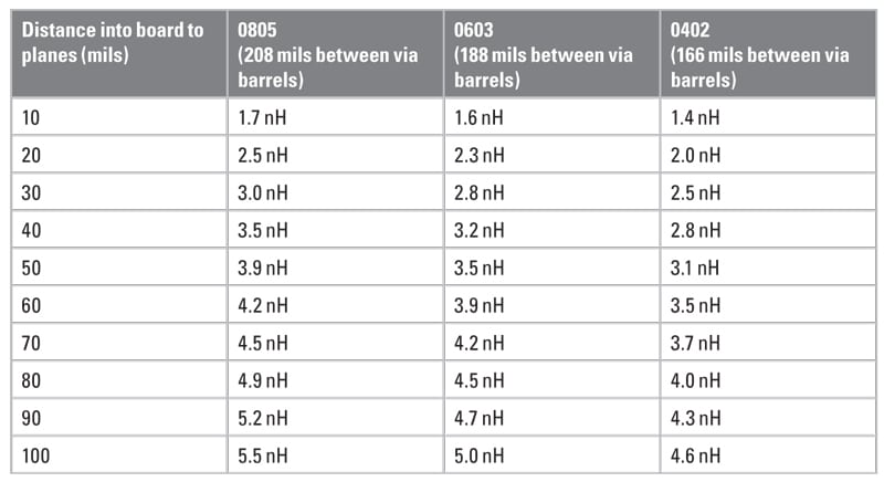
The connection inductance depends on the distance between the vias which connect the capacitor to the planes, and the distance from the top (or bottom) mounting location to the planes that are to be decoupled. [2] Figure 1 shows a side view of the typical capacitor mounting on a PCB. Table 1 shows some calculated [3] connection inductances (without ESL) for 0805, 0603, and 02 size SMT capacitors. [2-3]

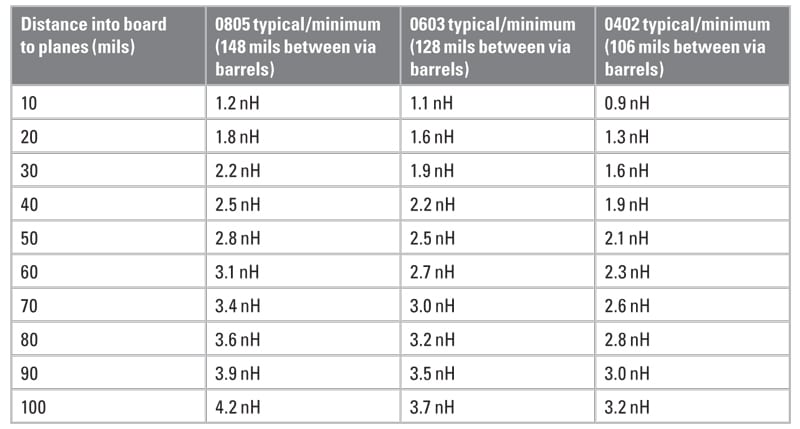
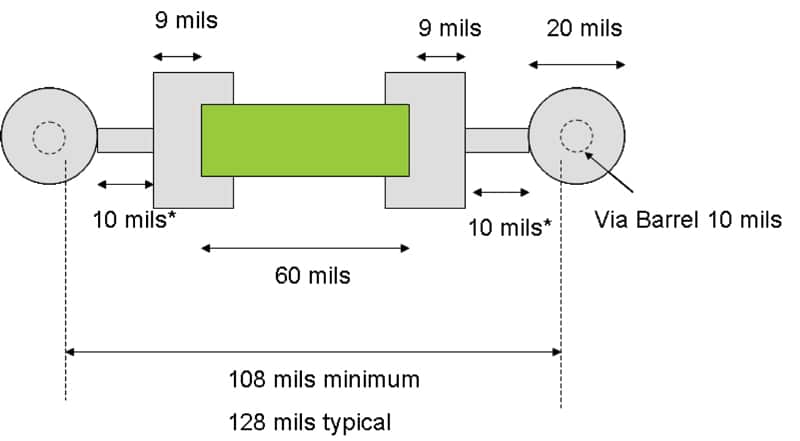
These values are calculated with the example of 7-8 mils from capacitor-to-mounting-pad-edge, 20 mils from capacitor-mounting-pad-edge-to-via-pad, via pad diameter of 20 mils, via barrel size of 10 mils, and trace width equal to 20 mils. The absolute minimum distance from the via pad to capacitor mounting pad edge is reported to be 10 mils, but typically 20 mils is used to be “safe.” Figures 2 and 3 show the 0603 and 0402 size capacitor mounting, respectively.

RESULTS
The results in Figures 4–13 show the impedance between the planes for both 5 mil and 10 mil spacing between the planes. The inductance includes both the connection inductance and the capacitors specified ESL.
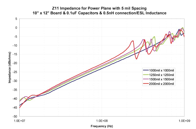
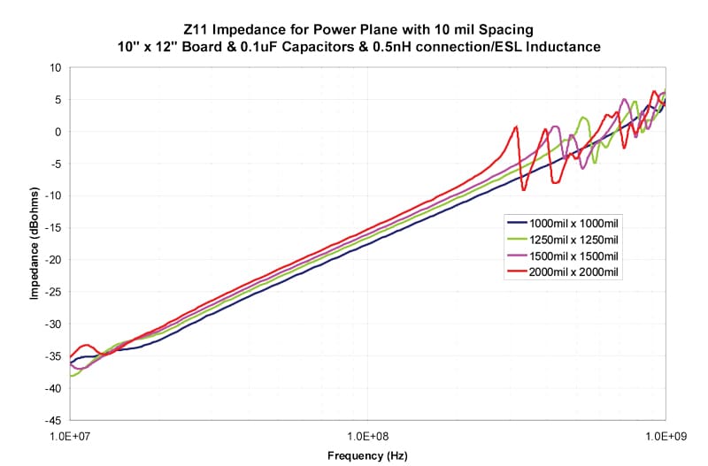
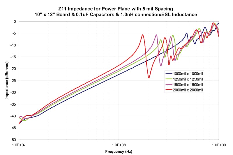
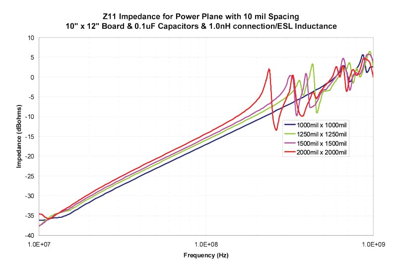
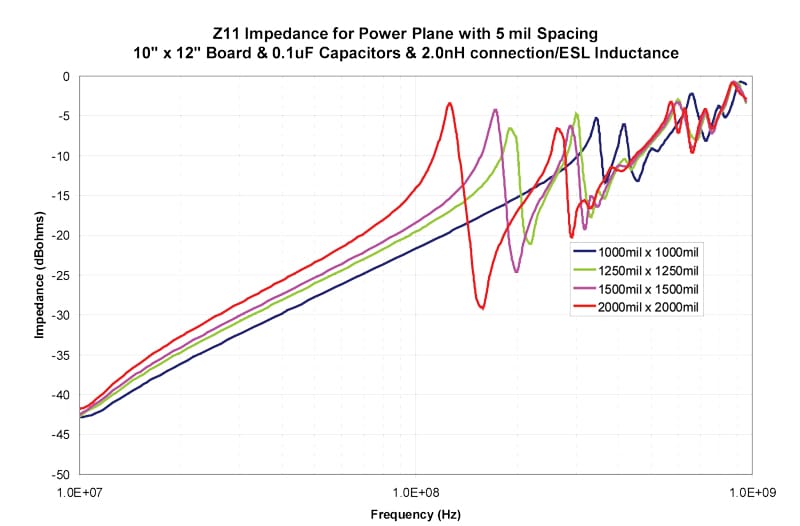
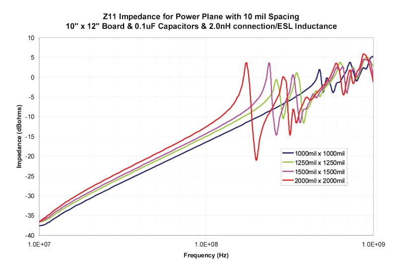
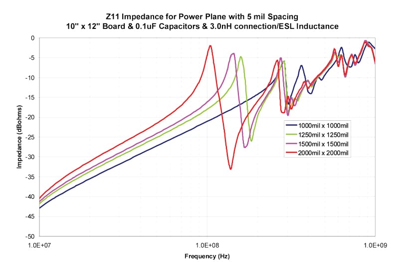
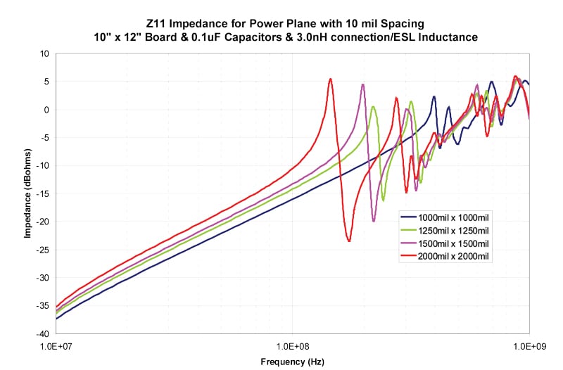
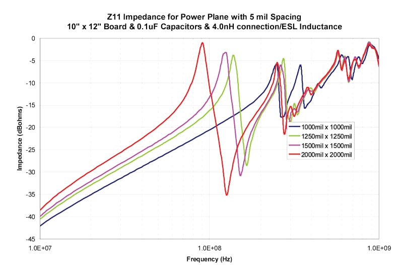
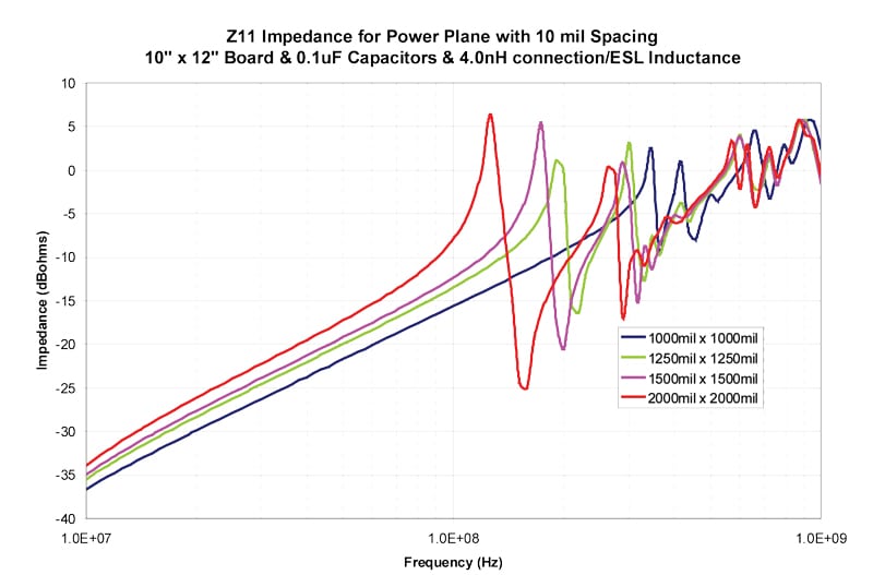
Table 2 shows the first resonant frequency for 5 mil spacing between the planes and Table 3 shows the frequency where the impedance rises above 0.1 ohms (-20 dBohms4). Table 4 shows the first resonant frequency for 10 mil spacing between the planes and Table 5 shows the frequency where the impedance rises above 0.1 ohms (-20 dBohms). Since the primary goal to avoid resonances is to maintain a low impedance, 0.1 ohms is chosen as a low impedance target. The actual target impedance may vary depending on the specific product.


Table 1 should be used together with Tables 2-5 to find the frequency where a grid density is no longer effective.
For example, in the case of a PCB stackup using 5 mil spacing between the planes and a pair of planes that are 10 mils from the top of the PCB, when 0603 size capacitors are used, the expected connection inductance is 1.1 nH. When a typical ESL of 0.5 nH is added we have total inductance of 1.6 nH. The expected first resonant frequency would be about 400 MHz for a 1000 x 1000 mil grid and about 200 MHz for a 1500 x 1500 mil grid.
However, if the same pair of planes are deeper into the PCB stackup, and the distance to the planes becomes 50 mils, the expected connection inductance becomes 2.5 nH. When ESL is added, the total inductance for the capacitor is 3.0 nH. The expected first resonant frequency would be about 280 MHz for a 1000 x 1000 mil grid and about 75 MHz for a 1500 x 1500 mil grid.
If the distance between the via pad edge and the capacitor pad edge is increased to 50 mils on each side, the resulting inductance values are shown in Table 6. With the exception of plane pairs close to the surface, the inductance can be seen to increase by more than 1 nH over the similar cases in Table 1. Once the value of inductance is determined, the effective range of the decoupling capacitor grid density is seen in Tables 2-5.
CONCLUSION
It can be easily seen that the effect of connection inductance (and ESL) limits the effectiveness of decoupling capacitors, especially when the grid density is relaxed to larger spacing. If the design goal is to have no resonances below 100–200 MHz, then a smaller grid density must be used, and even then, depending on the depth of the plane pair in the PCB stackup, the grid density may not be effective.
The depth of the plane pair in the PCB stackup shows when the decoupling capacitors should be mounted on the top of the PCB, and when it is more effective to mount them on the bottom of the PCB. When the pair of planes is deep in the PCB stack up, there will be less connection inductance when the capacitors are mounted on the bottom side of the PCB.
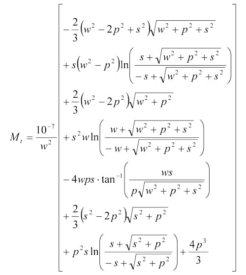
APPENDIX 1: Formula for Calculating Connection Inductance for Decoupling Capacitor
(A.1a)
(A.1b)
(3.21a)
(A.1c)
(A.1d)
(A.1e)
(A.1f)
s – separation between two vias
hs – height of the capacitor from the nearest power or ground plane
w – width of the trace connecting two vias, or width of the capacitor package if no trace
r – radius of the via
p – 2hs
For all the equations above, the dimensions are in meters, and the inductances are in Henrys.
REFERENCES
[1] www.ems-plus.com
[2] Knighten, James L., Bruce Archambeault, Jun Fan, Samuel Connor, James L. Drewniak, “PDN Design Strategies: II. Ceramic SMT Decoupling Capacitors – Does Location Matter?,” IEEE EMC Society Newsletter, Issue No. 208, Winter 2006, pp. 56-67. (www.emcs.org)
[3] Fan, Jun, Wei Cui, James L. Drewniak, Thomas Van Doren, and James L. Knighten, “Estimating the Noise Mitigating Effect of Local Decoupling in Printed Circuit Boards,” IEEE Trans. on Advanced Packaging, Vol. 25, No. 2, May 2002, pp. 154-165.
ABOUT THE AUTHOR
Bruce Archambeault is an IBM Distinguished Engineer at IBM in Research Triangle Park, NC. He received his B.S.E.E degree from the University of New Hampshire in 1977 and his M.S.E.E degree from Northeastern University in 1981. He received his Ph. D. from the University of New Hampshire in 1997. His doctoral research was in the area of computational electromagnetics applied to real-world EMC problems.
In 1981 he joined Digital Equipment Corporation and through 1994 he had assignments ranging from EMC/TEMPEST product design and testing to developing computational electromagnetic EMC-related software tools. In 1994 he joined SETH Corporation where he continued to develop computational electromagnetic EMC-related software tools and used them as a consulting engineer in a variety of different industries. In 1997 he joined IBM in Raleigh, N.C. where he is the lead EMC engineer, responsible for EMC tool development and use on a variety of products. During his career in the U.S. Air Force, he was responsible for in-house communications security and TEMPEST/EMC related research and development projects.
Dr. Archambeault has authored or co-authored a number of papers in computational electromagnetics, mostly applied to real-world EMC applications. He is currently a member of the Board of Directors for the IEEE EMC Society and a past Board of Directors member for the Applied Computational Electromagnetics Society (ACES). He has served as a past IEEE/EMCS Distinguished Lecturer and Associate Editor for the IEEE Transactions on Electromagnetic Compatibility. He is the author of the book “PCB Design for Real-World EMI Control” and the lead author of the book titled “EMI/EMC Computational Modeling Handbook.”


