A system’s immunity can be enhanced without causing any functional drawbacks.
Mart Coenen, EMCMCC bv, Eindhoven, the Netherlands
INTRODUCTION
With today’s digital designs and the time frame available for design-in, electrical system engineers and PCB designers are more or less forced to follow the application concepts provided by embedded device manufacturers. The information provided in the data sheets and application notes is likely to be followed verbatim in an effort to minimize any likelihood of failing functionally— i.e., to avoid expensive and time-consuming redesign. The next step in the system level requirements is not a primary concern.
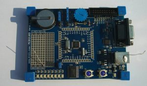
Most new microcontrollers are supplied in a multi-pin design. One should note the difference between the digital and analog peripherals and the digital core, which typically runs at a lower supply voltage. The core and peripheral supplies are often combined with an embedded low drop out (LDO) regulator only in ultra low-pin (ULP) count devices.
A few measures can be incorporated into the circuit design that are “selectable” later in the PCB application. An application can be further optimized by leaving some zero-Ohm resistors in the open position. With experience and increased confidence, product designers can incorporate these alternative techniques in future designs.
ROOT CAUSES
Typically, the RF emission from a microcontroller application stems from the digital core and the oscillator as the peripheral I/O will be characterized by less data transfer than the digital core. The digital core may run on the harmonics of the X-TAL oscillator frequency determined by the PLL (phase locked loop) settings during boot-up initiation so that the root cause of the RF emission is easily detected. In cases where the oscillator’s signal is fully symmetric, the X-TAL oscillator circuit will emit only its odd harmonics. With a slight error in the duty cycle, the even harmonics of the oscillator will pop up occasionally at the higher frequencies—typically above the 10th harmonic.
Just as the internal digital core clock frequency will differ from the X-TAL oscillator frequency, the same condition holds true with regard to the dominant odd harmonics of the symmetric core clock signals generated by the PLL. When dual or quad phase clocks are used, these will also show up externally as a dominant 2nd and/or 4th harmonic of the clock frequency used in the RF emission spectrum.
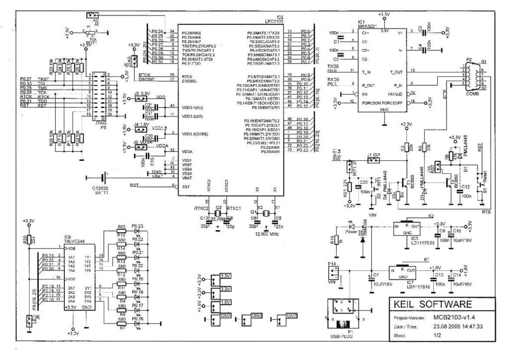
The principal cause of this RF emission is reliance on a design or application that forces RF currents to run off-chip. In the example of the oscillator, even in low swing applications, the output signal of the X-TAL oscillator is not fully sinusoidal. As the X-TAL will only pass a fraction of the fundamental frequency signal, all other output signal current will be dumped into the ground reference of the PCB by the load capacitance at the output of the oscillator. Using integrated on-chip load capacitors can prevent these off-chip currents of the oscillator circuit, and any RF emission will be caused by the X-TAL’s supply current. By utilizing a series resistance or inductance in the X-TAL supply (when separated by design), this RF emission contribution can be significantly decreased.
With LPCs (low pin counts), the supply current for the oscillator is taken from either the peripheral supply or the core supply; and as a result, the supply noise from the oscillator will be superimposed on all the I/Os or on the core. Also, the jitter of the oscillator will then be proportional with the data activity on the I/O ports or core as the internal oscillator’s supply voltage varies. Adding a series resistance with the oscillator’s output will generally reduce the RF peak current (increase output impedance) into the ground reference and will also reduce the crosstalk to the peripheral supply or core. For other applications, the oscillator’s supply voltage is internal taken from the peripheral or core supply via an internal RC-filter as the oscillator circuitry draws only a few mA.
The LPC ARM digital core on a KEIL evaluation board is conventionally decoupled using an off-chip capacitance of 100 nF that, in this particular application, is in parallel with an on-chip core capacitance of 4.4 nF (measured and biased at the nominal supply voltage) and from the point of off-chip decoupling (Figure 1). It has 25 nH in total with 3.14 Ω of loss resistance at higher frequencies.
From this digital ARM core circuit, a resonance frequency can be found at 15.2 MHz that is rather close to the X-TAL oscillator’s frequency of 12 MHz. The resonance quality is rather poor when it is assumed that the off-chip decoupling capacitance is considered as an RF short-circuit. Enlarging the off-chip capacitance or placing a few decoupling capacitors in parallel will have no effect on this resonance situation. Enlarging the off-chip series inductance of the core supply will lower the overall resonance frequency so that it becomes even more problematic as it nears 12 MHz, but it will improve significantly at a lower frequency. The use of a 1-µH lossy ferrite bead (SMD) in series with the digital core supply will bring the resonance frequency down to 2.5 MHz; a step that, in turn, will lower the current at 12 MHz by 10 dB or more. A significant RF emission reduction of 32 dB can be achieved with a series Impedance of 1 µH—i.e., 40 times the 25 nH that had been measured in the application. (These figures assume no parasitic bypasses.)
A SIMPLE MEASUREMENT TECHNIQUE
The formal RF emission measurement techniques discussed here are described in the IEC 61967-x series. For those interested in RF immunity, references can be found in IEC 62132-x and the IEC 62215 series that deals with immunity testing for transient disturbances.
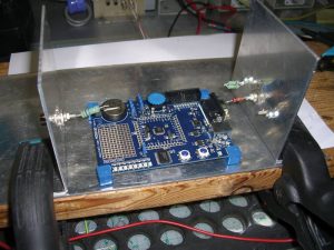
As many of the test boards, such as the one used in this instance, are a non-standardized size, the introduction of a cheap and very flexible test set-up is presented. In IEC 61967-5, the measurement test set-up uses a workbench Faraday cage (WBFC). In the product-related standard IEC 61000-4-6, Figure 7, there is information about the calibration of test jigs. Two of those L-shaped calibration test jigs can be used to build the RF emission test set-up. Other equipment needed includes just two additional 100-Ω resistors with short leads and a small metal reference plane that is to be fitted underneath the board being tested. Using two mechanical spring clamps, the L-shapes are forced onto the reference plane, (Figure 3). The 100-Ω resistors are placed from the left (patch area) and right side (USB shell) of the evaluation board using the BNC connectors at each side (see Figure 1 for the test port connections). At the two BNC-ports, the RF emissions can be measured at either side while the other port has been RF terminated with 50Ω. In most applications, these settings will be close to equal, but it is advisable to regard the maximum RF emission from both ports as a measure of RF emission.
MEASURES AND RESULTS
First, a common ground reference plane is constructed on the PCB that combines all grounds; digital, analog, USB, RS232, ISP, etc. The rationale behind this step is that the RF currents from each microcontroller circuit area will be confined and/or restricted. Equivalent measures for current confinement with other active devices on the board should be applied.
In this case, to obtain the relevant information from the evaluation board, all other activities – LED drive, RS232, and USB have been deactivated.
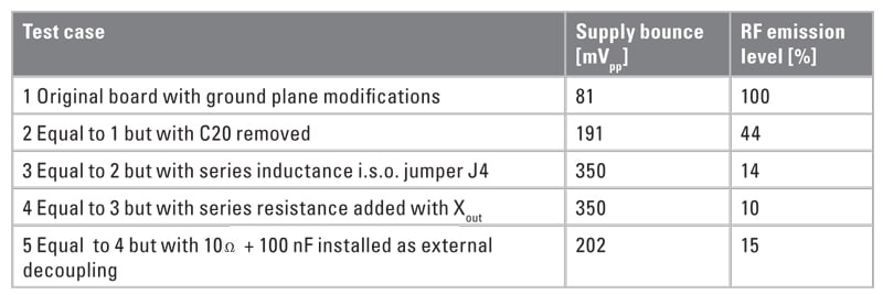
- Add series inductance with the digital core supply of the ULP ARM; add 1-µH inductance at J4 position and remove jumper. This step will be effective only in combination with measure 2. The inductance can be by-passed by the jumper
- Because of the chance of off-chip decoupling capacitances on the RC-network; remove C20 completely, or place RC-network—e.g., 10Ω + 100 nF (= tantalum capacitor). The higher the resistance, the better the current confinement will be at that supply node at the cost of dV/dt. As long as the peak-to-peak voltage swing (AC) remains less than 20 percent of the nominal supply voltage (1.8 Volt in this case, thus 360 mVpp), the device reliability will not be affected (CMOS090 and older processes). With new nanometer microprocessors, the supply variance tolerances are tighter, typically limited to 10 percent peak-to-peak.
- Add series resistance of 220 – 470Ω with the X-TAL output of the oscillator; X2, pin 12 of the device. This step lowers the RF current into the ground reference plane and will also lower the internal RF ripple on the X-TAL oscillator supply. Still, this step is irrelevant when the oscillator’s supply is taken from an internal source, or when on-chip oscillator capacitors have been used.
NOTE: Adding a series resistor with the oscillator’s output is also useful with level controlled oscillators but should not be used when the oscillator is used in overtone mode.
Five tests were performed, and results are listed below. For the sake of reliability, the core supply voltage was measured at 200 MHz bandwidth at 1 G/s with a resistive 10:1, 500-Ω RF probe. The envelope peak-to-peak voltage (worst case) over the program period has been recorded and is given in Table 1.
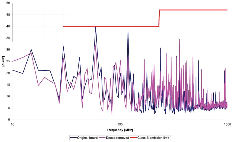
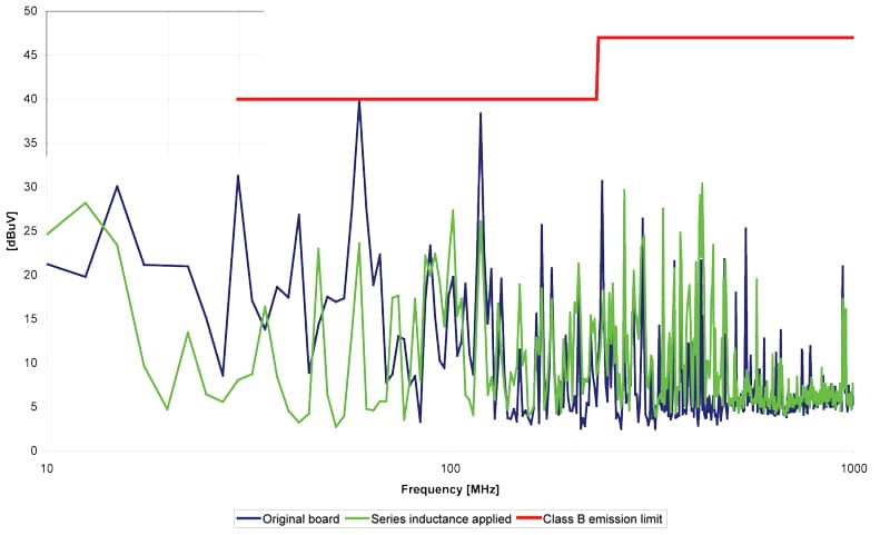
Sequentially, the RF emission from the board has been recorded by means of an RF spectrum analyzer with a 10-kHz bandwidth. The 10 kHz bandwidth was chosen to enable measurement of fixed harmonic signals and comparison of data. In Figure 4, the RF emission from the original board (case 1) is given in combination with case 2. As reference, the Class B emission limit line is drawn too, which is just met with the original board and its application.
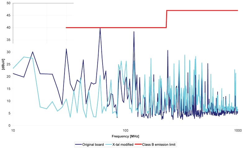
As can be seen from the Figures 4 and 5, the RF emission in the lower frequencies; 24 to 240 MHz, where the margin was low compared to the class B emission limit, a substantial RF emission reduction (> 15 dB) was possible. The RF emission at the higher frequencies can be further reduced by modifying the oscillator (Figure 6). Having implemented these measures, the supply voltage requirements with regard to the reliable operation of the device were still met (Table 1). Furthermore, all supply bounce now occurs at the Vddcore side and remains just at, or below, the requirements of IC processes involving this device. Overall, the modified board will now meet the Class B requirements by 12 dB or more over all the frequency ranges of interest with only minor changes in the bill of materials (BoM).
NOTE: The high level of RF emission at the end of the spectrum in the 900-MHz region in Figures 4 – 6 was produced by mobile telephone devices and reflects the fact that an RF open test bench set-up has been used.
CONCLUSIONS
Conventional application of modern microcontroller and other active devices with integrated decoupling measures (supplied by most silicon vendors) can be ineffective with regard to controlling RF emissions. Unfortunately, guidance for improved applications is seldom given. Employing RF current confinement and/or reduction techniques, one common PCB ground reference plane can be used to enhance the system’s immunity without causing any functional drawbacks. In fact, with a change of a few components, RF emissions can be reduced by 15 to 20 dB at critical frequencies without compromising the reliable operation of the devices.
NOTE: In changing an application and its RF current paths, some spectral emission lines might have increased slightly.
ACKNOWLEDGEMENT
This study was made possible with the support of NXP Regional Sales Support Europe in Eindhoven including test materials and the exchange of information. Special thanks to Kees Jansen and Kees van Seventer.
REFERENCES
[1] KEIL™ (An ARM® Company) evaluation board, type OM10079 + 598
[2] NXP LPC 2103 datasheets
[3] IEC 61967-5; Integrated circuits. Measurement of electromagnetic emissions, 150 kHz to 1 GHz. Measurement of conducted emissions. Workbench Faraday Cage method
[4] IEC 61000-4-6 Ed.2.2; Electromagnetic compatibility (EMC) – Part 4-6: Testing and measurement techniques – Immunity to conducted disturbances, induced by radio-frequency fields
[5] Coenen, Mart and Dick de Greef. “Optimized techniques for minimizing IR-drop and supply bounce.” Interference Technology EMC Test and Design Guide, November 2007.
[6] Coenen, Mart. “Off-chip decoupling measures: the EMC perspective.” Interference Technology EMC Directory and Design Guide.” May 2007.
ABOUT THE AUTHOR
Mart Coenen has over 29 years’ experience in EMC in various fields and has published many papers and publications. He has been actively involved in international EMC standardization since 1988 and was awarded with the IEC 1906. He is the former project leader of the standards IEC 61000-4-6 and IEC 61000-4-2 but has moved his focus towards EMC in integrated circuits. He was the former convenor of IEC TC47A/WG9 and, until last year, a member of WG2.
In addition to his former career with Phillips, he is a co-founder of the Dutch EMC/ESD Society and part-time lecturer of post-academic EMC courses. He also owns a private EMC consulting company.


