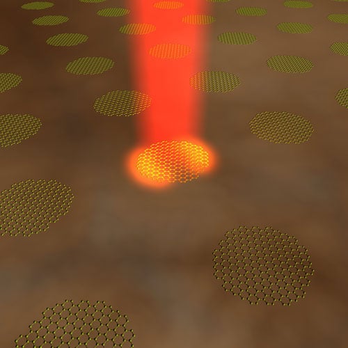
Physicists in Spain and the UK have calculated that graphene could be used to create a perfect absorber of light if it is doped and patterned into a periodic array. The work could lead to improved light-detection devices, particularly in the infrared part of the electromagnetic spectrum, where current technologies struggle to function.
The claim is extraordinary because conventional materials normally need to be thousands of atoms thick to absorb light completely.
The structure absorbs light by confining it to regions that are hundreds of times smaller than the wavelength of the light. This is done by exploiting plasmons that occur within the individual nanodisc structures. Plasmons are quantized collective oscillations of the electrons within a nanodisc – and they interact strongly with light.
Plasmons are more familiar to us in the high-frequency, visible part of the electromagnetic spectrum and notably in 3D metallic nanostructures. However, since graphene is only one atom thick and its electrons move in just two dimensions, plasmons in this material occur at much lower frequencies.
Light confinement in graphene is possible only if the material is electrically charged. And the wavelength at which light can be confined and absorbed depends on how much the material is charged. Also known as doping because it has an effect similar to that of introducing impurities to conventional semiconductors, charging is easily achieved by placing electrodes near the graphene. The amount of charging itself can then be controlled by varying the voltage applied to the electrodes.
In their calculations, the team studied how the patterned graphene absorbed light in the near- to mid-infrared range of the electromagnetic spectrum. The researchers say that it would be easy to extend their results to other wavelength ranges, towards the mid-infrared and the terahertz regime, for example, by directly applying the analytical equations that they employed.


